Cross-hair cell devices and methods for manufacturing the same

a cross-hair cell and cell technology, applied in the field of electronic devices, can solve the problems of increasing difficulty in operation and control of transistors, gate or other structure construction, and difficulty in construction

Active Publication Date: 2012-05-24
MICRON TECH INC
View PDF0 Cites 23 Cited by
  • Summary
  • Abstract
  • Description
  • Claims
  • Application Information

AI Technical Summary

Problems solved by technology

High aspect ratio fins typically are desirable but challenging to construct.
As the dimensions of the fin structures and the space between each fin are reduced, construction of gates or other structures, and operation and control of the transistors may be increasingly difficult.

Method used


Image

  • Cross-hair cell devices and methods for manufacturing the same
  • Cross-hair cell devices and methods for manufacturing the same
  • Cross-hair cell devices and methods for manufacturing the same

Examples


Embodiment Construction

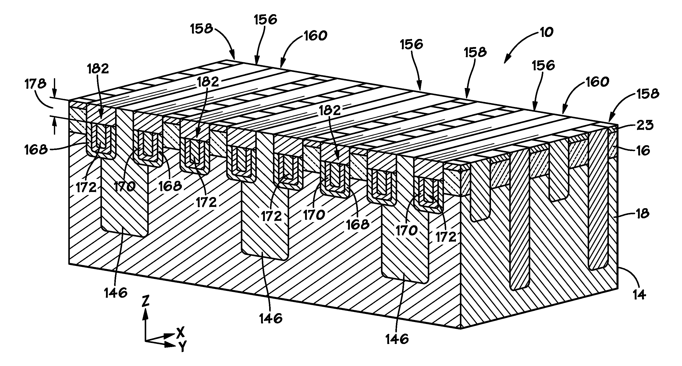
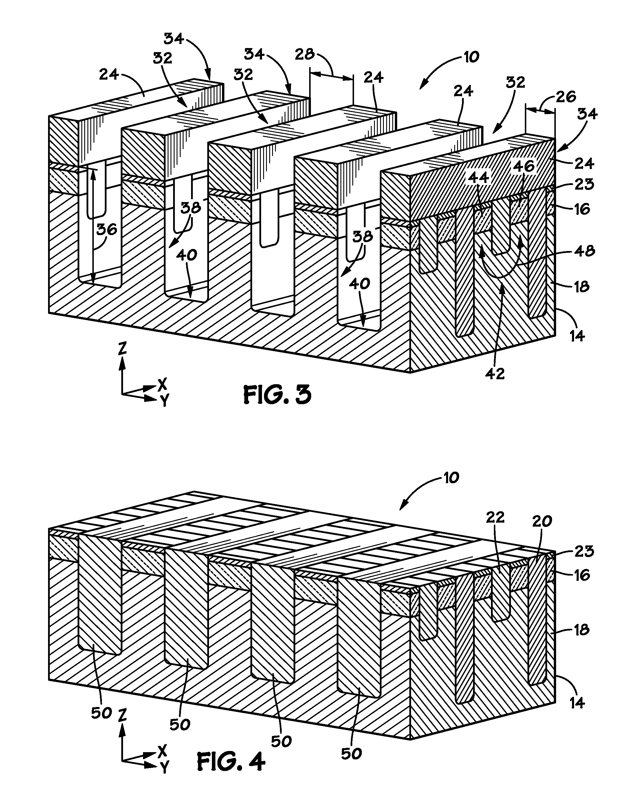
[0012]Some of the subsequently discussed embodiments may include processes for the manufacture of high aspect ratio structures such as finFETs having gates and, in some embodiments, grounded gates. As described in detail below, in one embodiment the process may include the formation of gate trenches and gates disposed on row trenches between fins, such that four gate trenches are formed for every two row trenches (i.e., for two pitches of the row trenches). In another embodiment, the process may include the fabrication of gate trenches, access line gates, and grounded gates, such that three gate trenches are formed for every two row trenches (i.e., for two pitches of the row trenches). The following discussion describes devices and process flows in accordance with embodiments of the present technique.

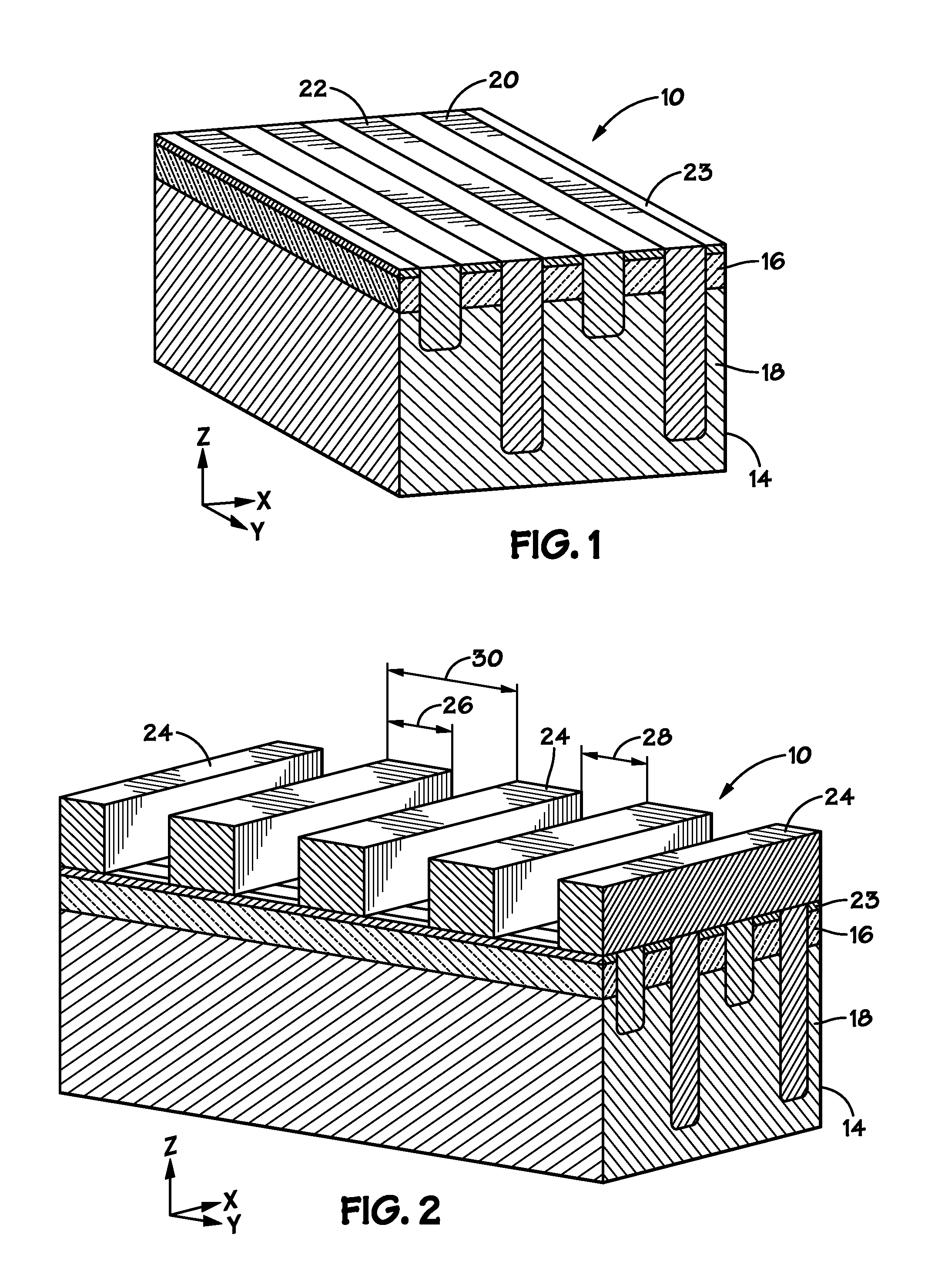
[0013]FIG. 1 depicts a cross-sectional plane view of a portion 10 of a memory array comprising high aspect ratio structures, e.g., fins, in accordance with an embodiment of the present ...


PUM


Abstract

Systems and methods are disclosed for manufacturing grounded gate cross-hair cells and standard cross-hair cells of fin field-effect transistors (finFETs). In one embodiment, a process may include forming gate trenches and gates on and parallel to row trenches in a substrate, wherein the gate trenches and gates are pitch-doubled such that four gate trenches are formed for every two row trenches. In another embodiment, a process may include forming gate trenches, gates, and grounded gates in a substrate, wherein the gate trenches and gates are formed such that three gate trenches are formed for every two row trenches.

Description

BACKGROUND[0001]1. Field of Invention[0002]Embodiments of the invention relate generally to electronic devices, and more specifically, to non-planar transistors and techniques for fabricating the same.[0003]2. Description of Related Art[0004]This section is intended to introduce the reader to various aspects of art that may be related to various aspects of the present invention, which are described and / or claimed below. This discussion is believed to be helpful in providing the reader with background information to facilitate a better understanding of the various aspects of the present invention. Accordingly, it should be understood that these statements are to be read in this light, and not as admissions of prior art.[0005]Fin field effect transistors (finFETs) are often built around a fin (e.g., a tall, thin semiconductive member) extending generally perpendicularly from a substrate. Typically, a gate traverses the fin by conformally running up one side of the fin over the top and...

Claims


Application Information

Patent Timeline
Patent Type & Authority Applications(United States)
IPC IPC(8): H01L27/092H01L21/302H01L21/18
CPCH01L21/823431H01L27/10879H01L27/10826H10B12/36H10B12/056
Inventor JUENGLING, WERNER
Owner MICRON TECH INC
Why Eureka
Try Eureka