Silicon dioxide film fabricating process

Active Publication Date: 2012-06-21
UNITED MICROELECTRONICS CORP
View PDF3 Cites 9 Cited by
  • Summary
  • Abstract
  • Description
  • Claims
  • Application Information

AI Technical Summary

Benefits of technology

[0004]Therefore, the object of the present invention is to provide a

Problems solved by technology

Conventionally, since the silicon dioxide film is formed on a silicon substrate by a

Method used


Image

  • Silicon dioxide film fabricating process
  • Silicon dioxide film fabricating process
  • Silicon dioxide film fabricating process

Examples


Example

[0018]The present invention will now be described more specifically with reference to the following embodiments. It is to be noted that the following descriptions of preferred embodiments of this invention are presented herein for purpose of illustration and description only. It is not intended to be exhaustive or to be limited to the precise form disclosed.

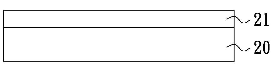
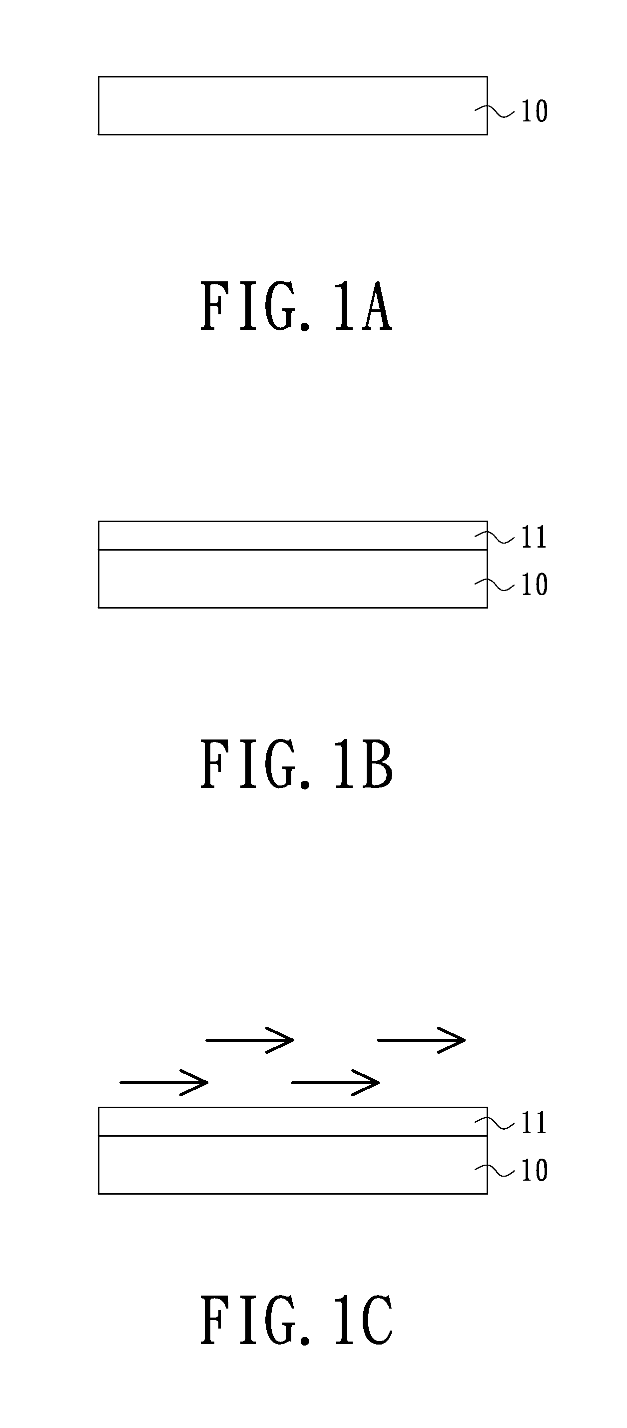
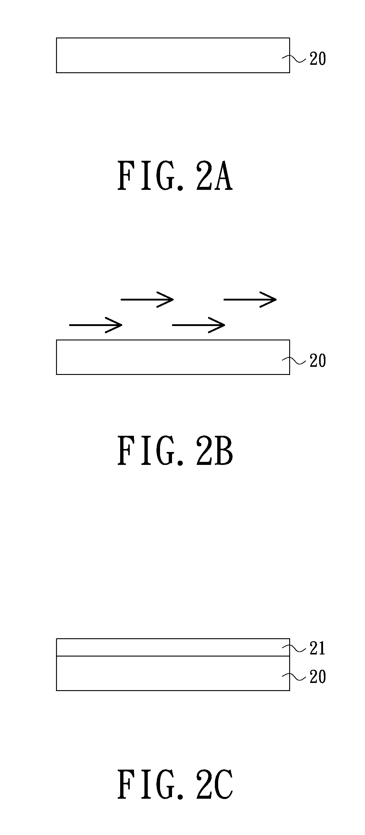
[0019]The present invention provides a silicon dioxide film fabricating process for fabricating a silicon dioxide film with good properties. FIGS. 1A, 1B and 1C are schematic views illustrating a silicon dioxide film fabricating process according to a first embodiment of the present invention. First of all, as shown in FIG. 1A, a substrate 10 is provided. An example of the substrate 10 is a silicon wafer. Then, a rapid thermal oxidation-in situ steam generation (RTO-ISSG) process is performed to form a silicon dioxide film 11 on the substrate 10 (see FIG. 1B). During the RTO-ISSG process is performed, a gas mixture of a hydrogen ...


PUM


Abstract

A silicon dioxide film fabricating process includes the following steps. Firstly, a substrate is provided. A rapid thermal oxidation-in situ steam generation process is performed to form a silicon dioxide film on the substrate. An annealing process is performed to anneal the substrate in a first gas mixture at a temperature in the range of 1000° C. to 1100° C.

Description

FIELD OF THE INVENTION[0001]The present invention relates to a silicon dioxide film fabricating process, and more particularly to a silicon dioxide film fabricating process applied to a semiconductor manufacturing process.BACKGROUND OF THE INVENTION[0002]In semiconductors, silicon dioxide films are widely used as insulating structures. For example, the gate insulator layers of metal-oxide-semiconductor (MOS) transistors or the floating gate insulator layers of electrically erasable programmable read-only memories (EEPROMs) are usually made of silicon dioxide. Recently, as the trend in designing integrated circuits is toward small-sized device dimensions, the thickness of the gate insulator layer is less than 100 angstroms. In other words, the electrical characteristics and the yield of the semiconductor components (e.g. transistors) are highly dependent on the quality of the silicon dioxide films. Conventionally, since the silicon dioxide film is formed on a silicon substrate by an ...

Claims


Application Information

Patent Timeline
IPC IPC(8): H01L21/316
CPCH01L21/02238H01L21/02312H01L21/28211H01L21/28185H01L21/28202H01L21/02337
Inventor LIN, CHIEN-LIANGWANG, YU-RENYEN, YING-WEI
Owner UNITED MICROELECTRONICS CORP
Why Eureka
Try Eureka