Substrate holder positioning method and substrate processing system

a substrate and positioning method technology, applied in semiconductor devices, electrical equipment, semiconductor/solid-state device testing/measurement, etc., can solve the problems of comparatively high cost of positioning devices, inability to achieve correct positioning in some cases, and inability to accurately position the substrate holder. , to achieve the effect of increasing the cost of the substrate holder

Active Publication Date: 2012-09-06
TOKYO ELECTRON LTD
View PDF11 Cites 45 Cited by
  • Summary
  • Abstract
  • Description
  • Claims
  • Application Information

AI Technical Summary

Benefits of technology

[0006]When the positioning device is employed, it is possible that the positioning device causes a positioning error unless the positioning device is inspected and calibrated frequently. If the positioning device is not properly handled, correct positioning cannot be achieved in some cases. The positioning device is comparatively expensive and, in some cases, a plurality of positioning devices suitable to the respective shapes of the processing modules to which substrates are carried are needed. Those positioning devices increase the cost of the substrate holder considerably. Therefore, it is desired to position the substrate holder without using any positioning device.

Problems solved by technology

When the positioning device is employed, it is possible that the positioning device causes a positioning error unless the positioning device is inspected and calibrated frequently.
If the positioning device is not properly handled, correct positioning cannot be achieved in some cases.
The positioning device is comparatively expensive and, in some cases, a plurality of positioning devices suitable to the respective shapes of the processing modules to which substrates are carried are needed.
Those positioning devices increase the cost of the substrate holder considerably.

Method used


Image

  • Substrate holder positioning method and substrate processing system
  • Substrate holder positioning method and substrate processing system
  • Substrate holder positioning method and substrate processing system

Examples


Embodiment Construction

[0033]Nonlimitative embodiments of the present invention will be described with reference to the accompanying drawings, in which the same or corresponding members or parts are designated by the same of corresponding reference characters and the duplicate description thereof will be omitted.

[0034]Coating and Developing System

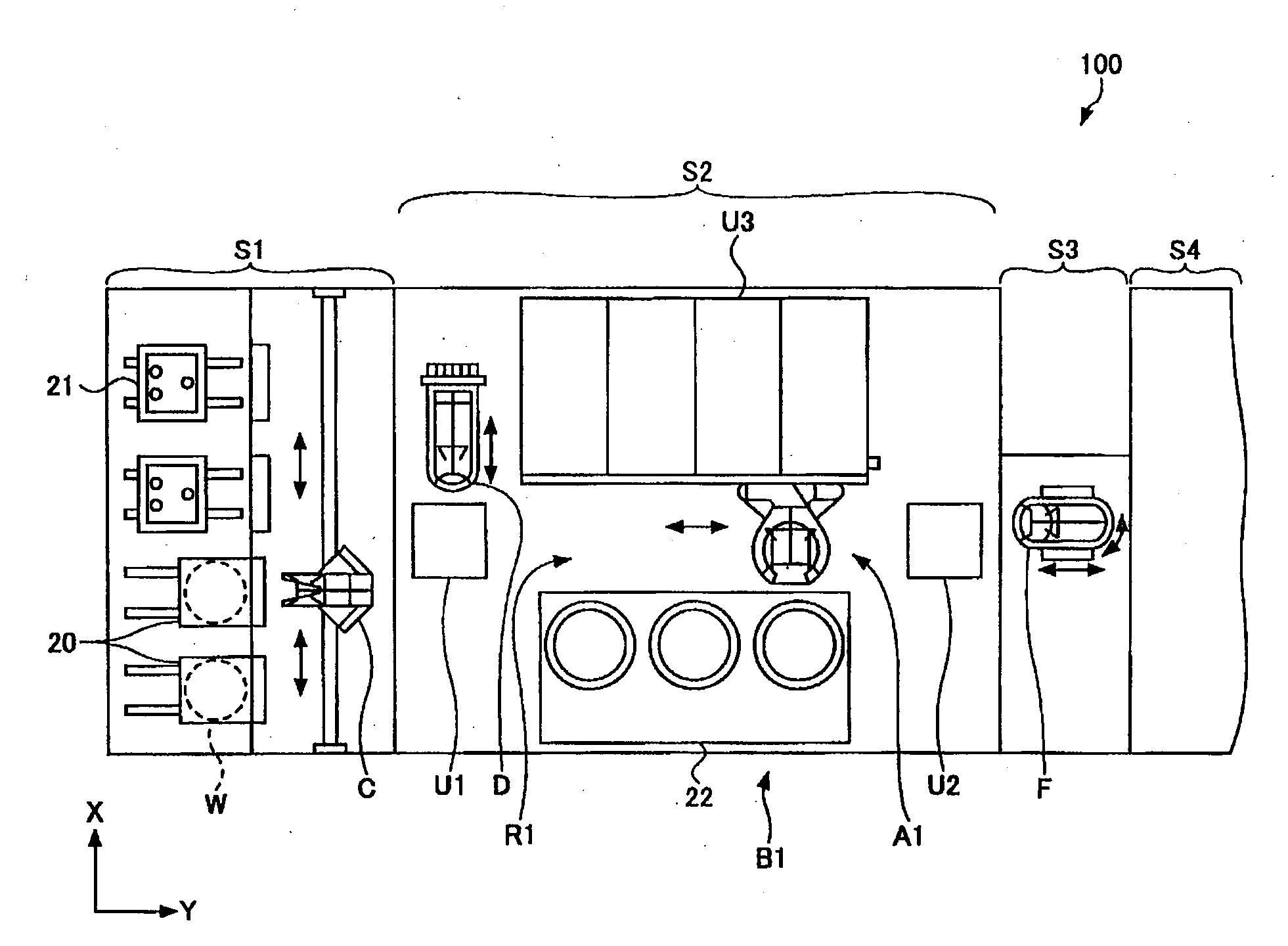
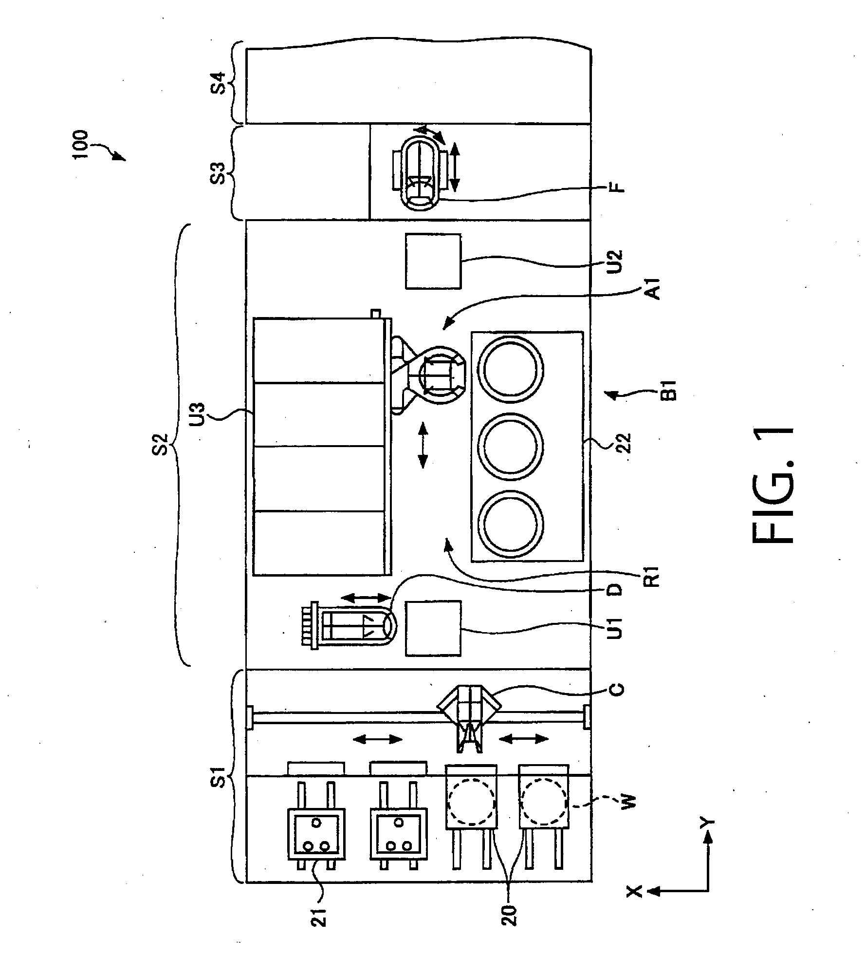
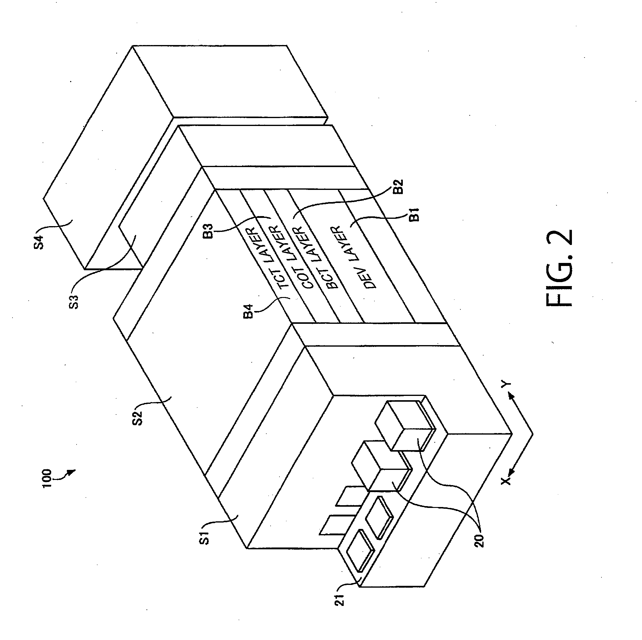
[0035]A coating and developing system 100 in a preferred embodiment of the present invention will be described with reference to FIGS. 1 to 4. Referring to FIGS. 1 and 2, the coating and developing system 100 has a carrier station S1, a processing station S2 and an interface station S3 arranged in that order. An exposure system S4 is connected to the interface station S3 of the coating and developing system 100.

[0036]The carrier station S1 is provided with support tables 21 and a carrying mechanism C. A carrier 20 containing a predetermined number of semiconductor wafers (hereinafter referred to simply as “wafer”) W is placed on the support table 21. In this embo...


PUM


Abstract

A substrate holder positioning method, capable of positioning a substrate holder without using any positioning jig, includes: measuring a first position of a substrate held on a substrate holder included in a substrate carrying mechanism; carrying the substrate held on the substrate holder to a substrate rotating unit for holding and rotating the substrate; turning the substrate held by the substrate rotating unit through a predetermined angle by the substrate rotating unit; transferring the substrate turned by the substrate rotating unit from the substrate rotating unit to the substrate holder; measuring a second position of the substrate transferred from the substrate rotating unit to the substrate holder; determining the position of the center of rotation of the substrate rotating unit on the basis of the first and the second position; and positioning the substrate holder on the basis of the position of the center of rotation.

Description

TECHNICAL FIELD[0001]The present invention relates to a substrate holder positioning method, and a substrate processing systemBACKGROUND ART[0002]A substrate processing system is used for fabricating semiconductor devices including flat panel displays (FPDs). The substrate processing system has processing modules and a substrate carrying mechanism for carrying a substrate from and to the processing modules. The substrate carrying mechanism of the substrate processing system delivers substrates sequentially to the processing modules. The processing modules process the substrates by predetermined processes, respectively. It is possible that the entire surface of the substrate cannot be uniformly processed unless the substrate is positioned correctly at a predetermined position in each processing module. Although the substrate carrying mechanism is constructed so as to exhibit high carrying accuracy, a positioning operation is essential to accurately positioning the substrate.[0003]A s...

Claims


Application Information

Patent Timeline
Patent Type & Authority Applications(United States)
IPC IPC(8): H01L21/68
CPCH01L21/6715H01L21/67748H01L21/681H01L21/68707H01L2924/0002H01L22/10H01L21/68H01L2924/00
Inventor DOUKI, YUICHIHAYASHI, TOKUTAROUIIDA, NARUAKIENOKIDA, SUGURU
Owner TOKYO ELECTRON LTD
Why Eureka
Try Eureka