
Method for making semiconductor structure

a technology of composite epitaxial layer and semiconductor structure, which is applied in the direction of semiconductor devices, electrical appliances, basic electric elements, etc., can solve the problems of reducing the critical dimension, and achieve the effect of sufficient gate channel stress and sufficient carrier mobility

Inactive Publication Date: 2013-05-16
UNITED MICROELECTRONICS CORP
View PDF6 Cites 1 Cited by
  • Summary
  • Abstract
  • Description
  • Claims
  • Application Information

AI Technical Summary

Benefits of technology

The present invention proposes a new method to create a composite epitaxial layer structure. This structure has the advantage of preventing the dopant in the epitaxial layer from diffusing back and also provides a sufficient gate channel stress. This means that the structure solves the issue of insufficient gate channel stress.

Problems solved by technology

In the process for manufacturing semiconductor elements, it is always a growing challenge for persons in the art to overcome, not only to constantly decrease the critical dimension but also to maintain the performance of the semiconductor elements.
One of the challenges is to maintain the carriers, i.e. electrons and electron holes, to have sufficient carrier mobility.
Although the recessed source and drain of a particular shape may further increase the stress on the gate channel, some adverse consequence, such as a short channel effect, happens when the dopant, such as B, in the doped epitaxial layer back diffuses into the gate channel.

Method used


Image

  • Method for making semiconductor structure
  • Method for making semiconductor structure
  • Method for making semiconductor structure

Examples


Embodiment Construction

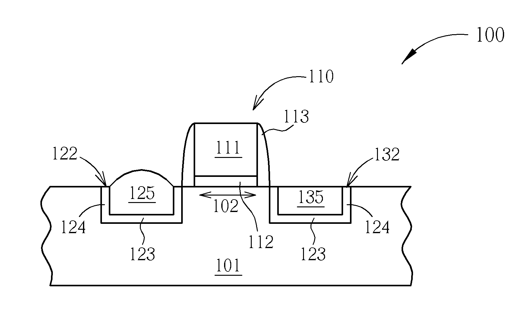
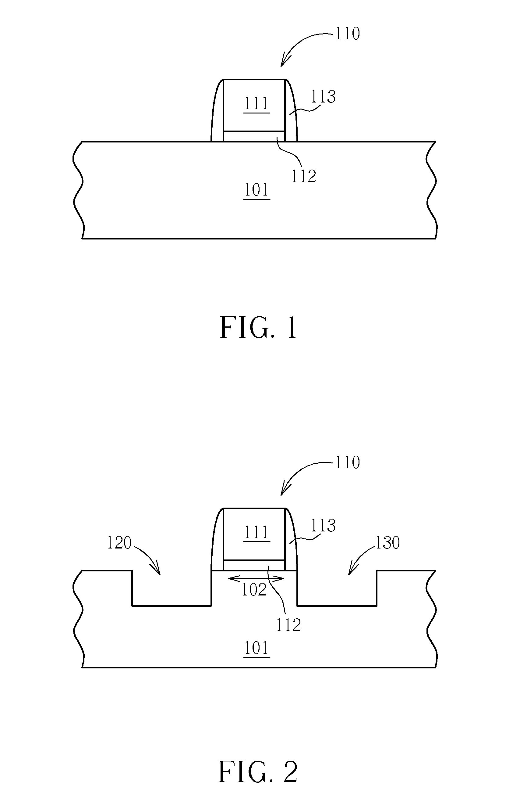
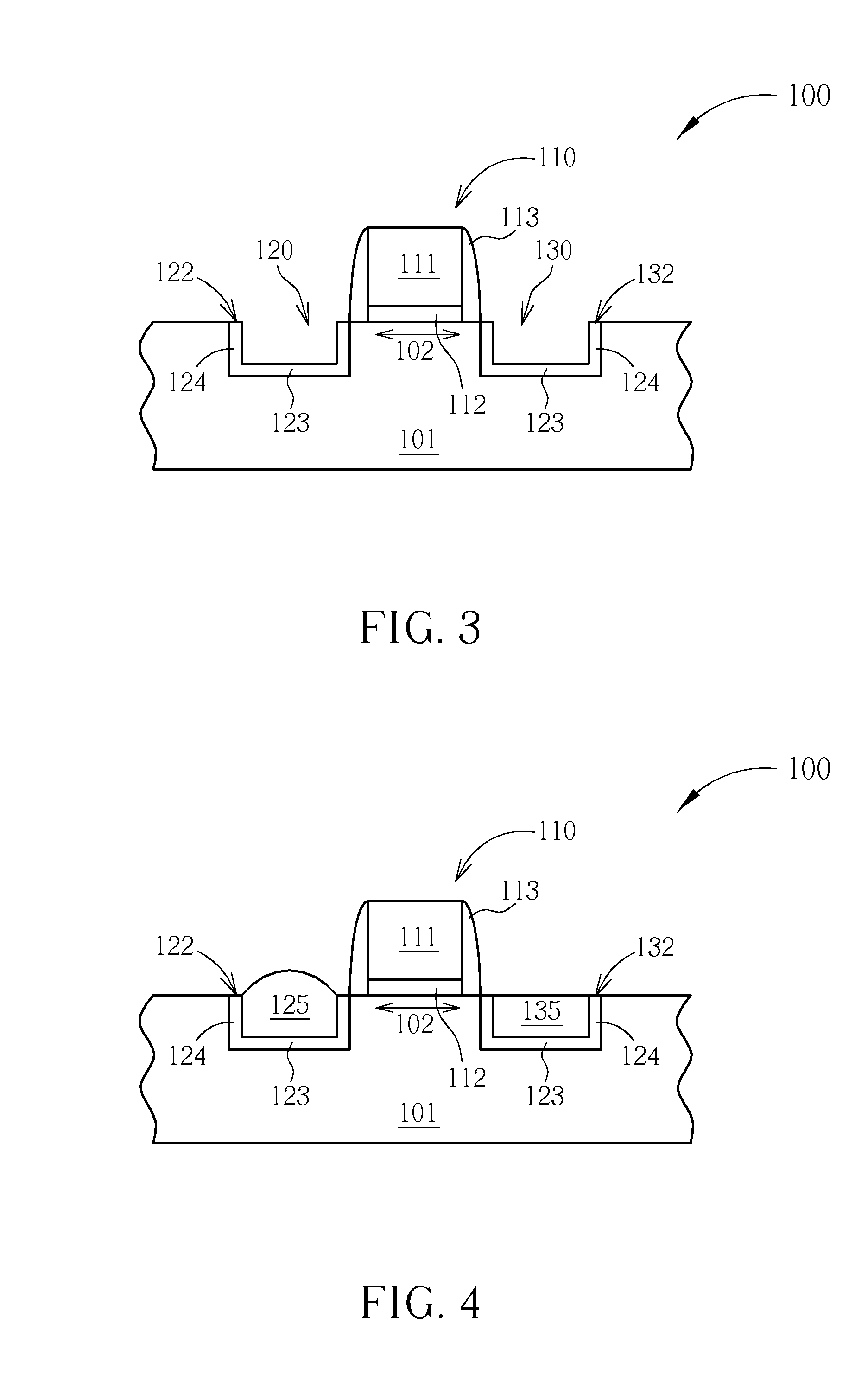
[0016]The present invention provides a semiconductor structure and the method for making the same. The semiconductor structure of the present invention has a non-doped epitaxial layer sticking to a recess and serving as a buffer layer. The doped epitaxial layer may block the back-diffusing of the dopant in the doped epitaxial layer. Besides, the non-doped epitaxial layer has a proper thickness ratio so the stress generated by the doped epitaxial layer is not compromised.

[0017]The present invention in a first aspect provides a method for making a semiconductor structure. FIGS. 1-5 illustrate an example for making the semiconductor structure of the present invention. Please refer to FIG. 1. First, a substrate 101 is provided. The substrate 101 is usually a semiconductor material, such as Si of a single crystal structure. Second, a gate structure 110 is formed on the substrate 101. The gate structure 110 may be formed on the substrate 101 by any conventional method, so that the gate st...


PUM

PropertyMeasurementUnit
semiconductor structureaaaaaaaaaa
flow rate ratioaaaaaaaaaa
shapeaaaaaaaaaa

Abstract

A method for forming a semiconductor structure is provided. First, multiple recesses are formed in a substrate. Second, a precursor mixture is provided to form a non-doped epitaxial layer on the inner surface of the recesses. The precursor mixture includes a silicon precursor, an epitaxial material precursor and a hydrogen-halogen compound. The flow rate ratio of the silicon precursor to the epitaxial material precursor is greater than 1.7. Later, a doped epitaxial layer including Si, the epitaxial material and the dopant is formed and substantially fills up the recess.

Description

CROSS REFERENCE TO RELATED APPLICATIONS[0001]This application is a divisional application of and claims the benefit of U.S. patent application Ser. No. 12 / 897,728, filed Oct. 4, 2010.BACKGROUND OF THE INVENTION[0002]1. Field of the Invention[0003]The present invention generally relates to a composite epitaxial layer structure and a method for forming the composite epitaxial layer structure. In particular, the present invention is directed to a composite epitaxial layer structure including a doped epitaxial layer and a non-doped epitaxial layer and a method for forming the composite epitaxial layer structure to ensure a stable electric property of a gate channel.[0004]2. Description of the Prior Art[0005]In the process for manufacturing semiconductor elements, it is always a growing challenge for persons in the art to overcome, not only to constantly decrease the critical dimension but also to maintain the performance of the semiconductor elements. One of the challenges is to maintai...

Claims


Application Information

Patent Timeline
Patent Type & Authority Applications(United States)
IPC IPC(8): H01L21/20
CPCH01L29/165H01L29/66636H01L21/20H01L29/7848H01L29/78
Inventor LIAO, CHIN-ILI, CHING-ICHAN, SHU-YEN
Owner UNITED MICROELECTRONICS CORP
Learn More