Semiconductor structure and method for making the same

Inactive Publication Date: 2012-04-05
UNITED MICROELECTRONICS CORP
View PDF3 Cites 4 Cited by
  • Summary
  • Abstract
  • Description
  • Claims
  • Application Information

AI Technical Summary

Benefits of technology

[0011]On one hand, due to the segregation of the non-doped epitaxial layer in the composite epitaxial layer structure of the present invention, the doped epitaxial layer does not contact the substrate at all, so the back-diffusing of the dopant in the doped e

Problems solved by technology

In the process for manufacturing semiconductor elements, it is always a growing challenge for persons in the art to overcome, not only to constantly decrease the critical dimension but also to maintain the performance of the semiconductor elements.
One of the challenges is to maintain the carriers, i.e. electrons and ele

Method used


Image

  • Semiconductor structure and method for making the same
  • Semiconductor structure and method for making the same
  • Semiconductor structure and method for making the same

Examples


Embodiment Construction

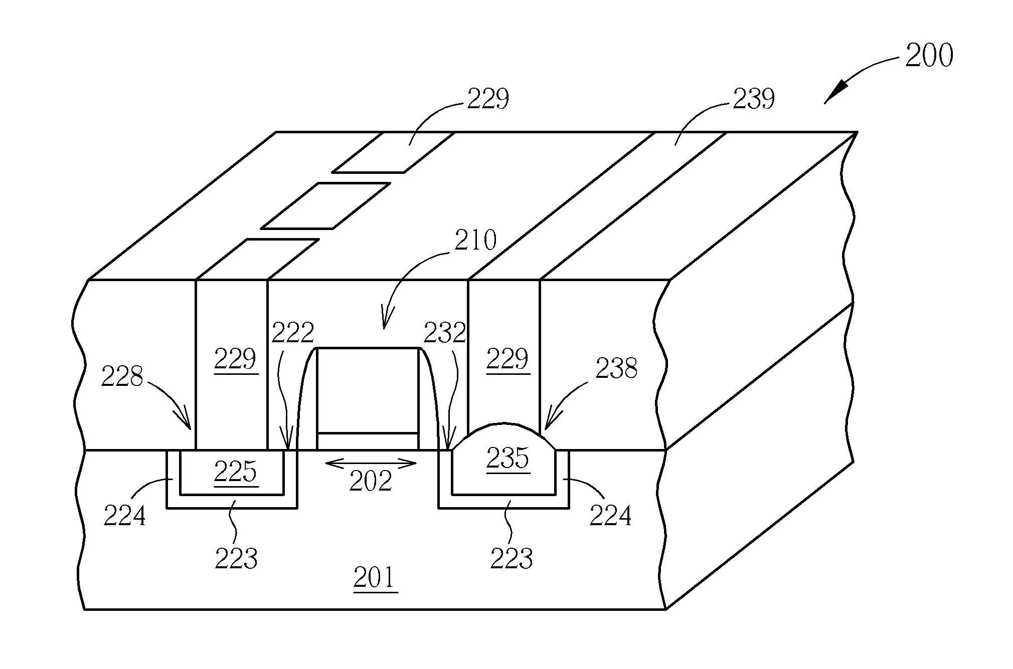
[0015]The present invention provides a semiconductor structure and the method for making the same. The semiconductor structure of the present invention has a non-doped epitaxial layer sticking to a recess and serving as a buffer layer. The doped epitaxial layer may block the back-diffusing of the dopant in the doped epitaxial layer. Besides, the non-doped epitaxial layer has a proper thickness ratio so the stress generated by the doped epitaxial layer is not compromised.

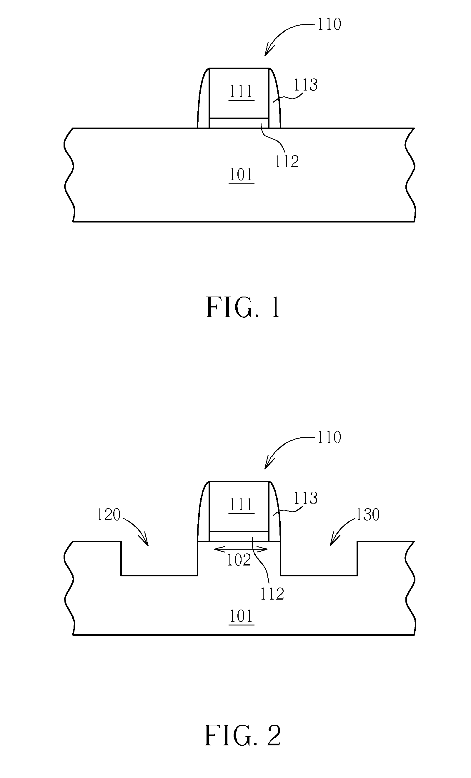
[0016]The present invention in a first aspect provides a method for making a semiconductor structure. FIGS. 1-5 illustrate an example for making the semiconductor structure of the present invention. Please refer to FIG. 1. First, a substrate 101 is provided. The substrate 101 is usually a semiconductor material, such as Si of a single crystal structure. Second, a gate structure 110 is formed on the substrate 101. The gate structure 110 may be formed on the substrate 101 by any conventional method, so that the gate st...


PUM


Abstract

A semiconductor structure includes a recess disposed in a substrate, a non-doped epitaxial layer and a doped epitaxial layer. The non-doped epitaxial layer is disposed on the inner surface of the recess and substantially consists of Si and an epitaxial layer. The non-doped epitaxial layer has a sidewall and a bottom which together cover the inner surface. The bottom thickness is not greater than 120% of the sidewall thickness. The non-doped epitaxial layer and the doped epitaxial layer together fill up the recess.

Description

BACKGROUND OF THE INVENTION[0001]1. Field of the Invention[0002]The present invention generally relates to a composite epitaxial layer structure and a method for forming the composite epitaxial layer structure. In particular, the present invention is directed to a composite epitaxial layer structure including a doped epitaxial layer and a non-doped epitaxial layer and a method for forming the composite epitaxial layer structure to ensure a stable electric property of a gate channel.[0003]2. Description of the Prior Art[0004]In the process for manufacturing semiconductor elements, it is always a growing challenge for persons in the art to overcome, not only to constantly decrease the critical dimension but also to maintain the performance of the semiconductor elements. One of the challenges is to maintain the carriers, i.e. electrons and electron holes, to have sufficient carrier mobility. It is already known that the carrier mobility in the gate channel of a MOS, such as a P-MOS or ...

Claims


Application Information

Patent Timeline
IPC IPC(8): H01L29/772H01L21/335
CPCH01L29/165H01L29/66636H01L21/20H01L29/7848H01L29/78
Inventor LIAO, CHIN-ILI, CHING-ICHAN, SHU-YEN
Owner UNITED MICROELECTRONICS CORP
Why Eureka
Try Eureka