Method of manufacturing semiconductor device, and semiconductor device

a manufacturing method and semiconductor technology, applied in the field of metal oxide semiconductors, can solve the problems of insufficient carrier mobility and achieve the effects of preventing short channel effect, reducing manufacturing costs, and reducing manufacturing costs

Active Publication Date: 2007-11-01
SONY CORP
View PDF1 Cites 263 Cited by
  • Summary
  • Abstract
  • Description
  • Claims
  • Application Information

AI Technical Summary

Benefits of technology

[0015]According to the semiconductor device as just-mentioned, the mixed crystal layer containing the impurity with a concentration gradient such that the impurity concentration increases along the direction from the silicon substrate side toward the surface. Therefore, the mixed crystal layer in the vicinity of the channel region, beneath the gate electrode, of the silicon substrate contains the impurity in a lower concentration as compared with that on the surface side. This ensures that the diffusion of the impurity from the mixed crystal layer due to a heat treatment is restrained, and the short channel effect is prevented from being generated. In addition, since it is unnecessary to enlarge the distance between the region beneath the gate electrode and the mixed crystal layer, a sufficient carrier mobility can be obtained.
[0016]As has been above-mentioned, according to the method of manufacturing a semiconductor device and the semiconductor device which pertain to the present invention, the short channel effect can be prevented from being generated, and a sufficient carrier mobility can be obtained, so that transistor characteristics can be enhanced.

Problems solved by technology

However, the above-mentioned method of manufacturing a semiconductor device has the following problem.
In that case, however, the stress exerted on the channel region 18 is weakened, so that a sufficient carrier mobility may not be obtained.

Method used


Image

  • Method of manufacturing semiconductor device, and semiconductor device
  • Method of manufacturing semiconductor device, and semiconductor device
  • Method of manufacturing semiconductor device, and semiconductor device

Examples


first embodiment

[0022]An embodiment of the method of manufacturing a semiconductor device pertaining to the present invention will be described below, taking the method of manufacturing a PMOSFET as an example and referring to the manufacturing step sectional diagrams in FIGS. 1A to 2G. Incidentally, in the following description, the same configurations as those described in the background of the invention above will be denoted by the same symbols as used above.

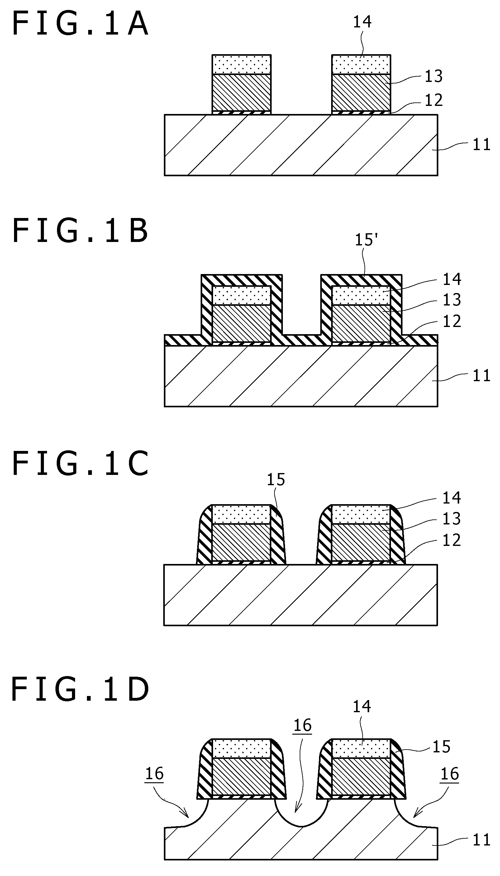
[0023]First, as shown in FIG. 1A, a silicon substrate 11 composed of single crystal silicon is prepared, and device isolation regions are formed on the face side thereof. In this case, for example, device isolation regions of the STI (shallow trench isolation) structure are formed, in which trenches are formed on the face side of the silicon substrate 11, and an insulating film composed of a silicon oxide film, for example, is buried in the trenches.

[0024]Next, on the silicon substrate 11 in each area isolated by the device isolation regions...

second embodiment

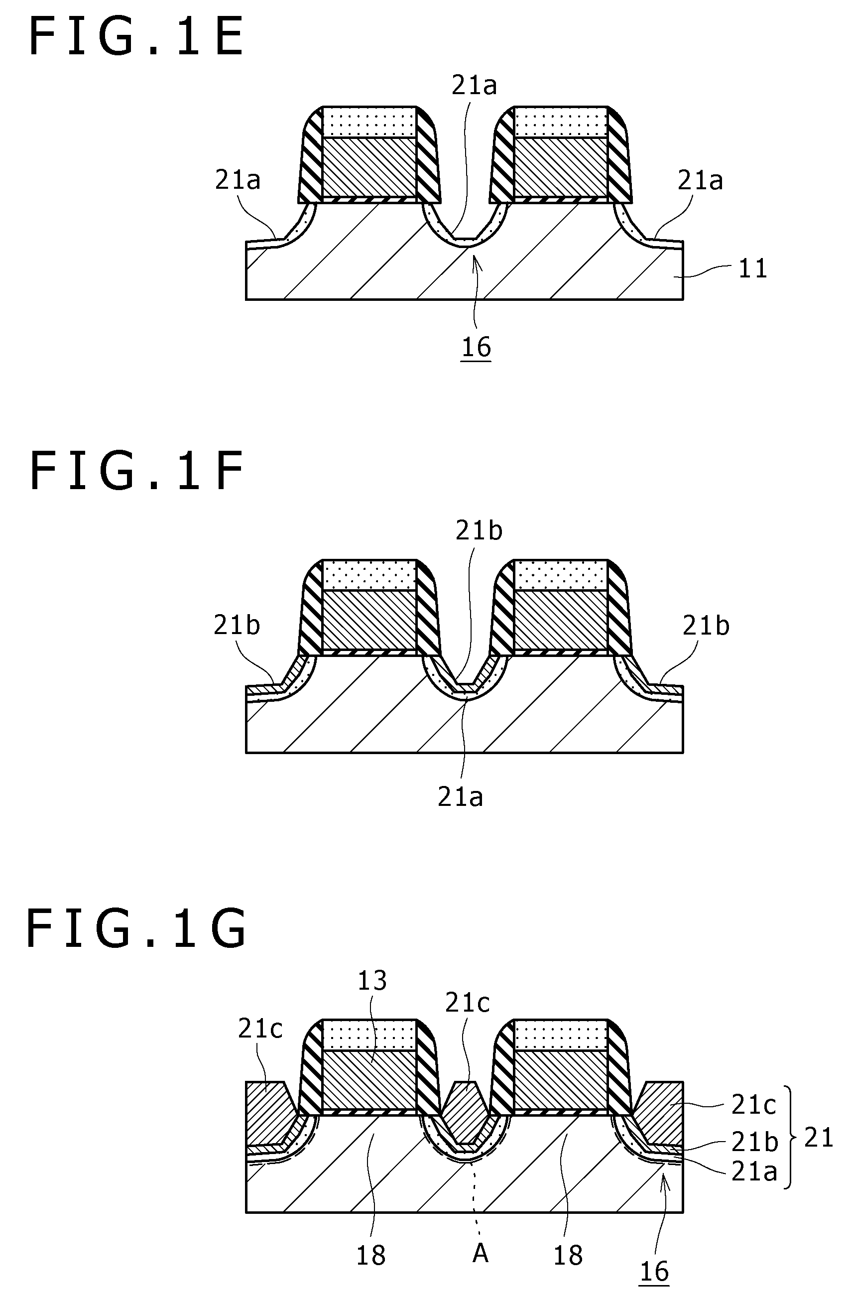
[0046]While the method of manufacturing a PMOSFET has been taken as an example in the description of the first embodiment above, in this embodiment a method of manufacturing an NMOSFET is taken as an example and description thereof will be made referring to FIGS. 2A to 2C. Incidentally, the steps up to the step of digging down the surface of a silicon substrate 11 are carried out in the same manner as the steps described referring to FIGS. 1A to 1D above.

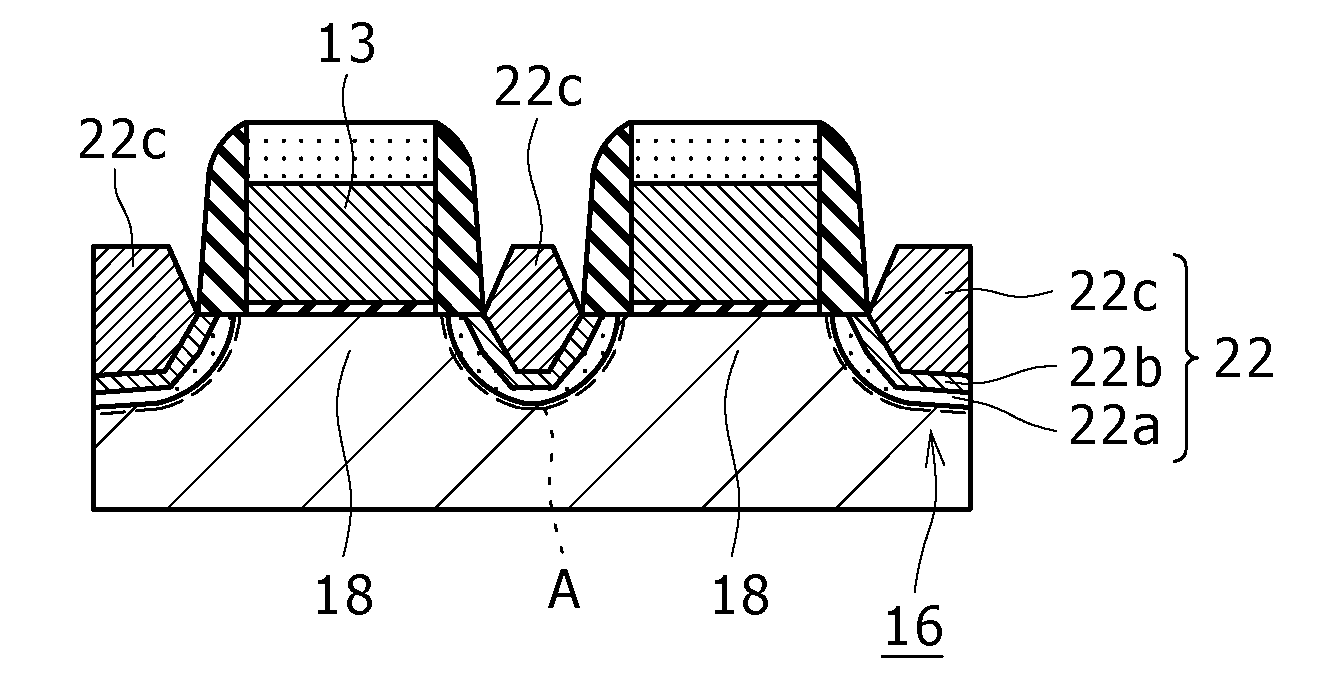
[0047]In the case of manufacturing an NMOSFET, first, as shown in FIG. 2A, a silicon-carbon (SiC) layer (mixed crystal layer) composed of silicon (Si) and atoms (C) smaller in lattice constant than silicon and containing, for example, arsenic (As) as an impurity is epitaxially grown on the surfaces of recessed regions 16, i.e., on the surfaces of the dug-down portions of the silicon substrate 11.

[0048]In this case, also, the SiC layer is epitaxially grown so as to contain As with such a concentration gradient that the As concentrati...

modified example 1

[0062]While an example in which As is contained as an impurity in the SiC layer for forming the source / drain regions of the NMOSFET has been described in the second embodiment above, phosphorus (P) may be used, in place of As, as the impurity.

[0063]In this case, also, the first SiC layer 22a is formed in a film thickness of one to 30 nm so as to contain P as the impurity in a concentration in the range of 1×10¹⁸ to 1×1019 cm−3.

[0064]As for the film forming conditions for the first SiC layer 22a, DCS, SiH3CH3 diluted with hydrogen (H2) to one vol %, HCl, and phosphorus hydride (PH3) diluted with H2 to 50 ppm are used as film-forming gases, at gas flow rates of DCS / SiH3CH3 / HCl / PH3=ten to 100 / one to 50 / ten to 100 / one to 150 (ml / min), a treating temperature of 650 to 750° C., and a treating pressure of 1.3 to 13.3 kPa.

[0065]Next, on the first SiC layer 22a, a second SiC layer 22b is formed in a film thickness of one to 20 nm so as to contain P as an impurity with such a concentration gr...


PUM

PropertyMeasurementUnit
thicknessaaaaaaaaaa
pressureaaaaaaaaaa
temperatureaaaaaaaaaa

Abstract

A method of manufacturing a semiconductor device includes: the first step of forming a gate electrode over a silicon substrate, with a gate insulating film; and the second step of digging down a surface layer of the silicon substrate by etching conducted with the gate electrode as a mask. The method of manufacturing the semiconductor device further includes the third step of epitaxially growing, on the surface of the dug-down portion of the silicon substrate, a mixed crystal layer including silicon and atoms different in lattice constant from silicon so that the mixed crystal layer contains an impurity with such a concentration gradient that the impurity concentration increases along the direction from the silicon substrate side toward the surface of the mixed crystal layer.

Description

CROSS REFERENCES TO RELATED APPLICATIONS[0001]The present invention contains subject matter related to Japan Patent Application JP 2006-121605 filed with the Japan Patent Office on Apr. 26, 2006, the entire contents of which being incorporated herein by reference.BACKGROUND OF THE INVENTION[0002]1. Field of the Invention[0003]The present invention relates to a method of manufacturing a semiconductor device and the semiconductor device, particularly to a MOS (Metal Oxide Semiconductor) type field effect transistor.[0004]2. Description of the Related Art[0005]In recent years, for the purpose of enhancing the performance of transistors, impressing of a stress on a channel region so as to increase the drain current has been investigated. Examples of the stress impressing method include a method in which a highly stressed film is formed after the formation of a gate electrode so as to impress a stress on a channel region, and a process in which the source / drain regions of a P-channel MOS...

Claims


Application Information

Patent Timeline
Patent Type & Authority Applications(United States)
IPC IPC(8): H01L21/84
CPCH01L29/165H01L29/66628H01L29/7848H01L29/7834H01L29/66636
Inventor MIYANAMI, YUKI
Owner SONY CORP
Why Eureka
Try Eureka