Method of manufacturing resistor

a manufacturing method and resistor technology, applied in the direction of resistor details, lamination ancillary operations, chemistry apparatus and processes, etc., can solve the problems of high cost of using electron beams, x-ray generation of electron beams, and inability to weld electrode materials and resistance materials with laser beams, etc., to enhance laser welding intensity, and large thickness

Active Publication Date: 2013-05-30
CYNTEC
View PDF1 Cites 2 Cited by
  • Summary
  • Abstract
  • Description
  • Claims
  • Application Information

AI Technical Summary

Benefits of technology

[0012]As mentioned in the above, when a laser is used to weld a junction between the resistance material and the electrode material, the invention proposes that the beam area from the laser to the resistance material is larger than the beam area from the laser to the electrode material. Since the reflectivity of the resistance material is smaller than the reflectivity of the electrode material, the resistance material with smaller reflectivity absorbs more laser energy and then transmits heat to the electrode material. The heat, which is transmitted to the electrode material from the resistance material, can be used with laser energy absorbed by the electrode material to weld the electrode material and the resistance material well. Accordingly, the method of the invention is capable of enhancing laser welding intensity between the resistance material and the electrode material of the resistor effectively. Furthermore, the invention can selectively weld the junctions between the resistance material and the electrode materials by the laser from one or two sides of the resistance material according to different resistance materials with different thicknesses, so as to enhance laser welding intensity between the resistance material and the electrode material. Moreover, if the resistance material has a large thickness (e.g. larger than 1 mm), the method of the invention may use a laser with small spot size and large output power to weld the junctions between the resistance material and the electrode materials first and then use another laser with large spot size and small output power to re-weld the junctions between the resistance material and the electrode materials, so as to ensure that the junctions have enough welding intensity and good surface flatness.

Problems solved by technology

Since copper has high reflectivity, light cannot be absorbed by copper well so that laser cannot be used to weld electrode material and resistance material.
However, the electron beam has some disadvantages as follows: first, the electron beam must be used in a vacuum chamber; second, the cost of using the electron beam is high; third, the electron beam generates X-rays; and fourth, a tool used with the electron beam cannot be magnetic.

Method used


Image

  • Method of manufacturing resistor
  • Method of manufacturing resistor
  • Method of manufacturing resistor

Examples


Embodiment Construction

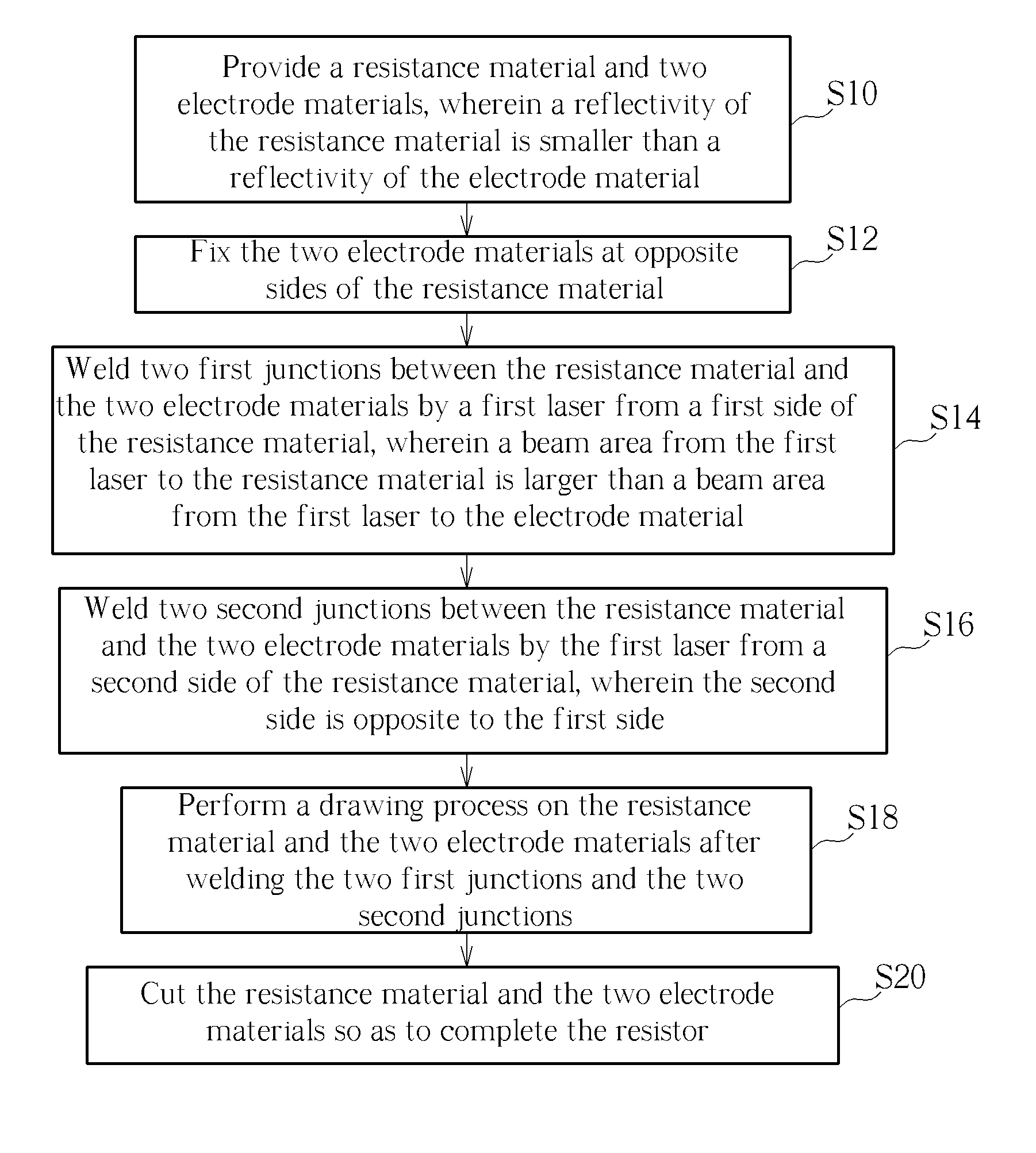
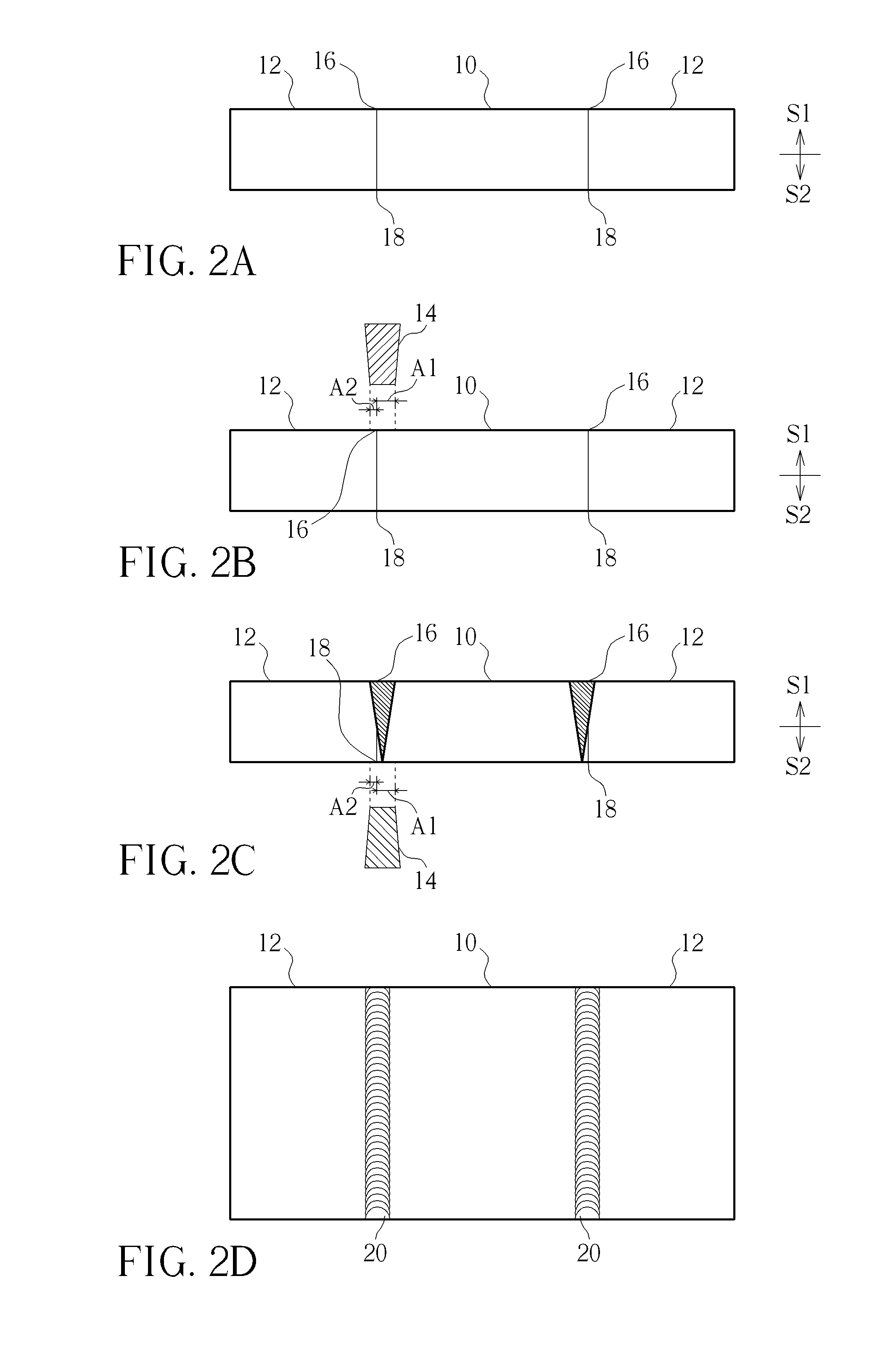
[0020]Referring to FIGS. 1 to 4, FIG. 1 is a flowchart illustrating a method of manufacturing a resistor according to an embodiment of the invention, FIGS. 2A to 2D are schematic diagrams illustrating processes associated with the method shown in FIG. 1, FIG. 3 is a perspective view illustrating a resistor 1 manufactured by the method shown in FIG. 1, and FIG. 4 is a perspective view illustrating the resistor 1 shown in FIG. 3 from another viewing angle. First of all, step S10 is performed to provide a resistance material 10 and two electrode materials 12 (as shown in FIG. 2A), wherein a reflectivity of the resistance material 10 is smaller than a reflectivity of the electrode material 12. In this embodiment, the resistance material 10 may be NiCu alloy, MnCu alloy, NiCr alloy, NiCrAlSi alloy, CuMnSn alloy and so on, and the electrode material 12 may be Cu, Cu coated solder and so on.

[0021]Afterward, step S12 is performed to fix the two electrode materials 12 at opposite sides of th...


PUM

PropertyMeasurementUnit
thicknessaaaaaaaaaa
thicknessaaaaaaaaaa
resistanceaaaaaaaaaa

Abstract

A method of manufacturing a resistor includes steps of providing a resistance material and two electrode materials, wherein a reflectivity of the resistance material is smaller than a reflectivity of the electrode material; fixing the two electrode materials at opposite sides of the resistance material; and welding two first junctions between the resistance material and the two electrode materials by a first laser from a first side of the resistance material, wherein a beam area from the first laser to the resistance material is larger than a beam area from the first laser to the electrode material.

Description

CROSS REFERENCE TO RELATED APPLICATIONS[0001]This application claims the benefit of U.S. Provisional Application No. 61 / 563,546, which was filed on Nov. 24, 2011, and is incorporated herein by reference.BACKGROUND OF THE INVENTION[0002]1. Field of the Invention[0003]The invention relates to a method of manufacturing a resistor and, more particularly, to a method capable of enhancing laser welding intensity between resistance material and electrode material of a resistor effectively.[0004]2. Description of the Prior Art[0005]A conventional resistor is manufactured by welding two electrode materials at opposite sides of a resistance material. In general, copper is chosen to be the electrode material. Since copper has high reflectivity, light cannot be absorbed by copper well so that laser cannot be used to weld electrode material and resistance material. In prior art, a continuous electron beam is proposed to be used to weld resistance material and copper electrode so as to manufactur...

Claims


Application Information

Patent Timeline
Patent Type & Authority Applications(United States)
IPC IPC(8): H01C17/28
CPCH01C1/144H01C17/28
Inventor LO, TA-WEN
Owner CYNTEC
Why Eureka
Try Eureka