Electro-Optical Single-Sideband Modulator

a single-sideband modulator and optical circuit technology, applied in the field of optical single-sideband modulators, can solve the problems of the approach to implement ssb modulation is usually quite complex in terms of internal configuration, operation, and external drivers, and the approach to implement ssb modulation is usually quite complex in terms of optical circuits with two nested mz-like structures, and potentially affecting the effect of optical fibers

Active Publication Date: 2013-06-06
SELEX SISTEMI INTEGRATI
View PDF1 Cites 11 Cited by
  • Summary
  • Abstract
  • Description
  • Claims
  • Application Information

AI Technical Summary

Benefits of technology

[0020]In broad outline, unlike the MZ-based approach adopted in the EOSSBMs of the prior art, where a proper phase relation is exploited between two π / 2 phase shifted modulating signals which simultaneously modulate the same optical carrier signal, and then the resulting two DSB modulated optical signals are caused to interfere to result in the unwanted side lobes being cancelled, the present invention is not based on a MZ approach and causes directly a simple shift of the incoming optical spectrum, with a small amount of shifted power and a large residual unshifted carrier.

Problems solved by technology

On the other hand, EOSSBMs are usually quite complex in their internal configuration, in their operation, and in the external drivers needed for their operation.
Nevertheless, this approach to implement SSB modulation clearly looks quite complex in term of optical circuit with two nested MZ-like structures, the one made up with optical fibers also being potentially affected by large thermo-mechanical instability and fluctuations.
In this architecture, as well as in the others mentioned above, at each recombination Y junction a partial destructive interference effect occurs, thus causing part of optical power being lost in radiative modes.

Method used


Image

  • Electro-Optical Single-Sideband Modulator
  • Electro-Optical Single-Sideband Modulator
  • Electro-Optical Single-Sideband Modulator

Examples


Embodiment Construction

[0024]The following discussion is presented to enable a person skilled in the art to make and use the invention. Various modifications to the embodiments will be readily apparent to those skilled in the art, without departing from the scope of the present invention as claimed. Thus, the present invention is not intended to be limited to the embodiments shown, but is to be accorded the widest scope consistent with the principles and features disclosed herein and defined in the appended claims.

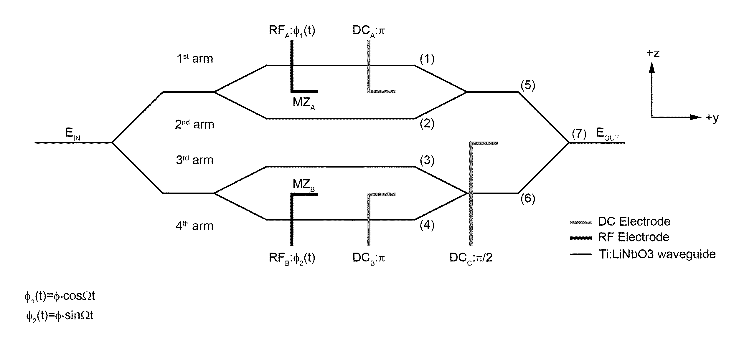
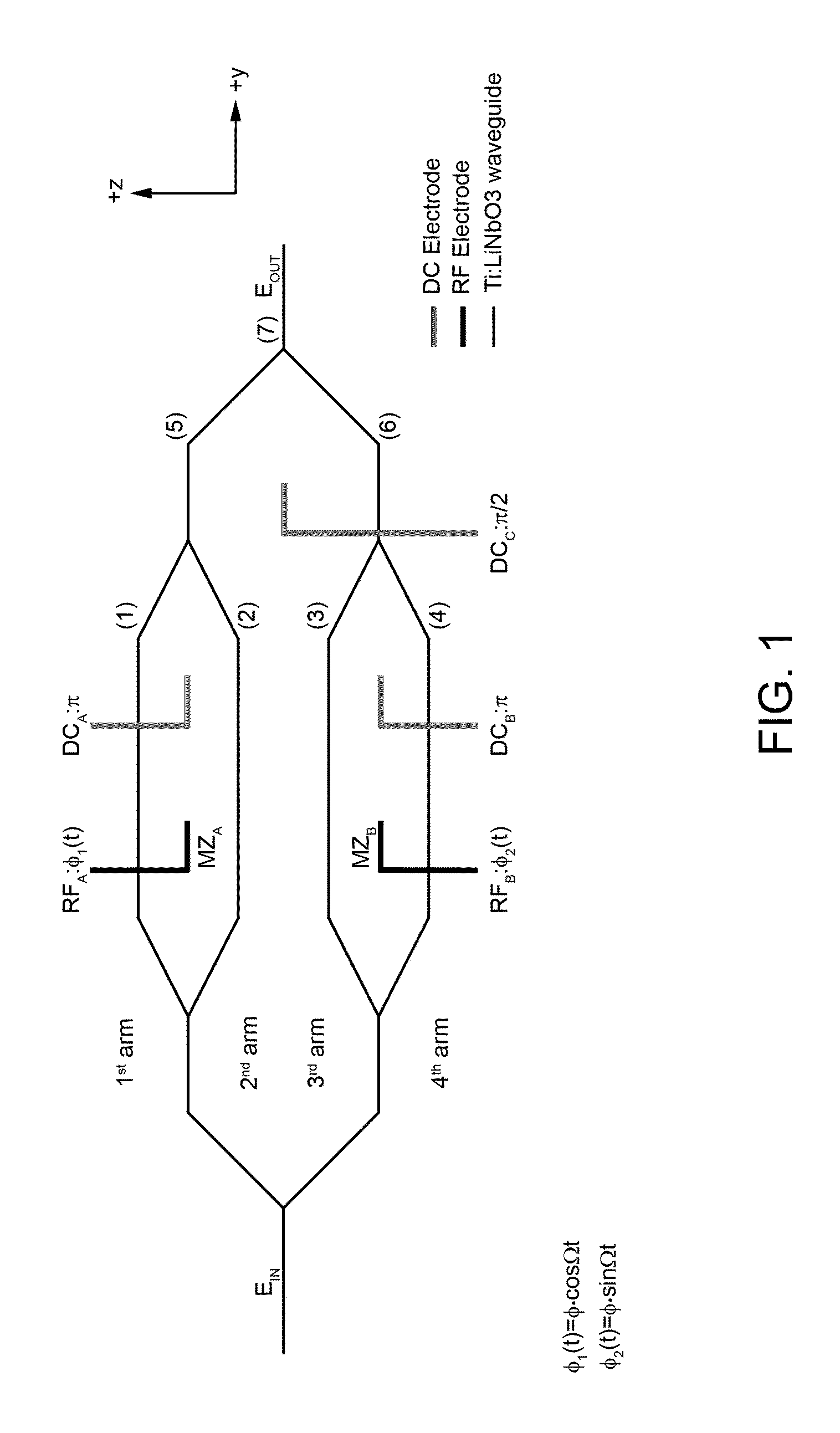
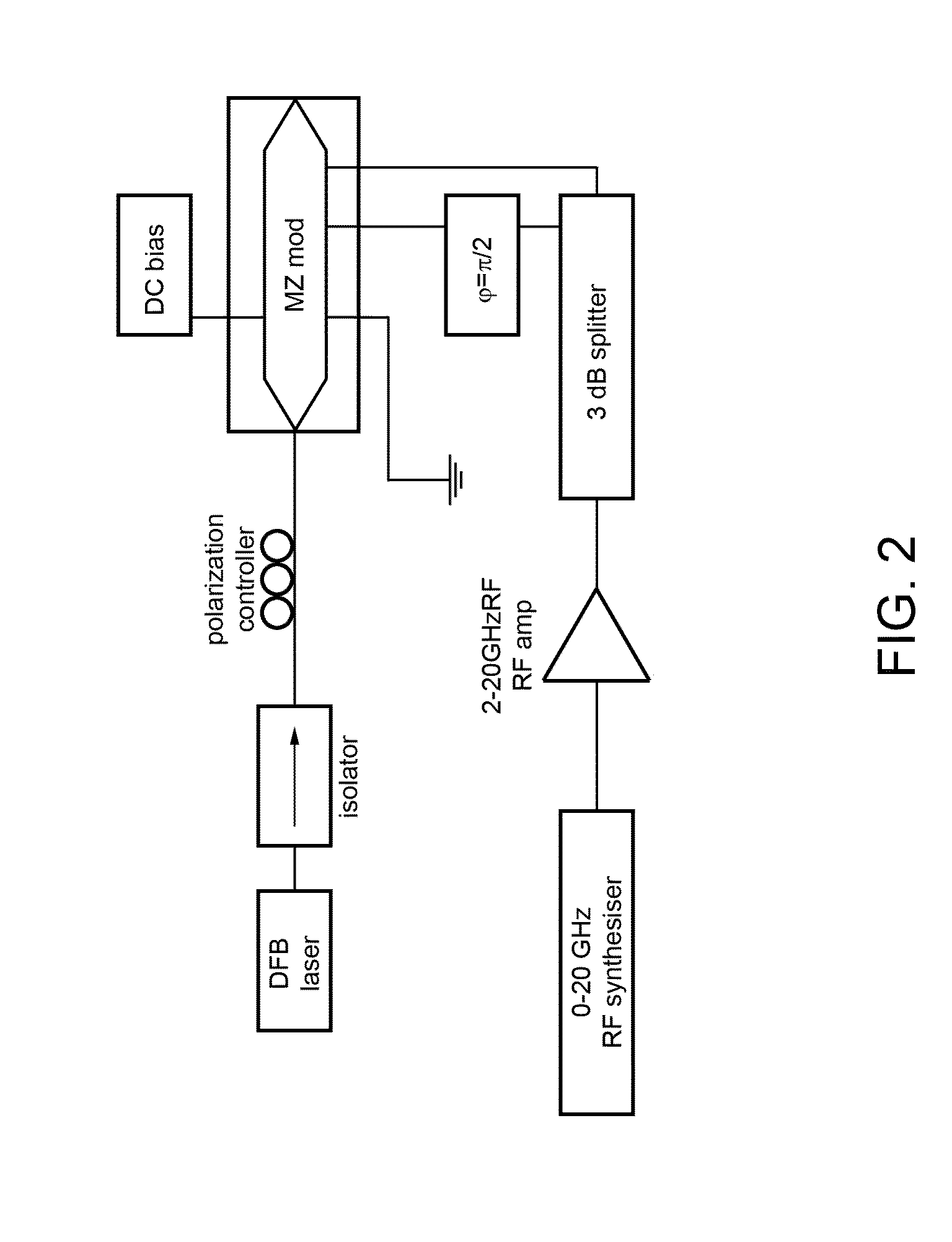
[0025]An EOSSBM according to the present invention is schematically depicted in FIG. 3 and generally referenced by reference numeral 1.

[0026]EOSSBM 1 basically includes:

[0027]an electro-optical substrate 2, conveniently an X-cut LiNbO3 substrate (other suitable electro-optical materials, different from LiNbO3 but still endowed with electro-optical properties, may be LiTaO3, KTP, GaAs, etc.);

[0028]a bimodal optical waveguide structure 3 formed in the substrate 2 in a conventional manner, for exam...


PUM


Abstract

An electro-optical single-sideband modulator comprising:
    • an electro-optical substrate;
    • a bimodal optical waveguide structure formed in the substrate to support different optical modes having associated optical frequencies and optical propagation constants and comprising an optical input to receive an input optical carrier signal having an optical frequency, and a pair of optical outputs to output corresponding SSB modulated optical signals, each having an optical frequency spectrum with a single side lobe; and
      • an electrode structure formed on the substrate to receive an input electrical modulating signal having an associated electrical frequency and electrical propagation constant, and to responsively apply an electrical field to the bimodal optical waveguide structure.

Description

TECHNICAL FIELD OF THE INVENTION[0001]The present invention relates in general to electro-optical modulators, and in particular to electro-optical single-sideband modulators (EOSSBMs).BACKGROUND ART[0002]As is known, electro-optical modulators are crucial optical components for optical digital and analog links for signal transmission and processing, in that they are capable of modulating optical power of optical carriers by means of driving electrical signals.[0003]EOSSBMs are especially useful in optical fiber communication systems, such as higher density wavelength multiplexing and long-haul fiber transmission due to reduced non-linear optical effects, because of reduced optical power.[0004]The presence of a single side lobe in the optical spectrum of a SSB-modulated optical signal results in several technical advantages, the main of which are half spectral occupation compared to standard Double SideBand (DSB) modulation and no fading of the optical signal at the end of an optical...

Claims


Application Information

Patent Timeline
Patent Type & Authority Applications(United States)
IPC IPC(8): H04B10/12
CPCH04B10/501G02F2201/05G02F1/3134G02F1/0356H04B10/5165
Inventor DISPENZA, MASSIMILIANOSECCHI, ALBERTORICCI, MASSIMOCASAGRANDE, STEFANOEVANGELISTI, ANDREAROVERE, FABIO DELLA
Owner SELEX SISTEMI INTEGRATI
Why Eureka
Try Eureka