Electro processor with shielded contact ring

Inactive Publication Date: 2013-06-13
APPLIED MATERIALS INC
View PDF5 Cites 21 Cited by
  • Summary
  • Abstract
  • Description
  • Claims
  • Application Information

AI Technical Summary

Benefits of technology

[0004]A new contact ring for an electro processor has now been invented which largely overcomes the challenges described above. The contact ring has a plurality of spaced apart contact fingers. In a first aspect, a shield at least partially overlies the contact fingers. The shield may be provided in the form of an annular ring substantially completely overlying an

Problems solved by technology

In dry contact ring processors, thin seed layers are prone to inadvertent etching due to seal leaking and/or residual chemistry on the seal.
Joule heating due to high currents passing through a thin seed layer can also be disruptive to uniform plating.
In wet contact ring processors, a thief electrode at the edge of the wafer may be needed to control the “terminal effect” which results in a non-uniform electric fie

Method used


Image

  • Electro processor with shielded contact ring
  • Electro processor with shielded contact ring
  • Electro processor with shielded contact ring

Examples


Example

DETAILED DESCRIPTION OF THE DRAWINGS

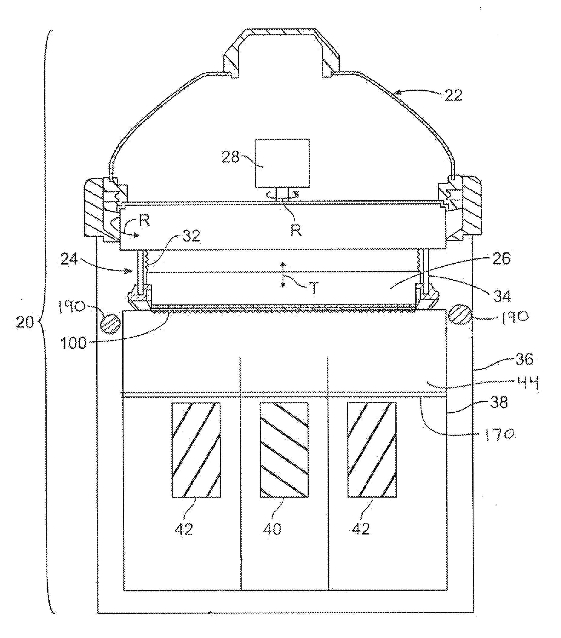
[0014]As shown in FIG. 1, and electro processing chamber 20 has a head 22 including a rotor 24. A motor 28 in the head 22 rotates the rotor 24, as indicated by the arrow R. A contact ring assembly 30 on the rotor 24 makes electrical contact with a work piece or wafer 100 held into or onto the rotor 24. The rotor 24 may include a backing plate 26, and ring actuators 34 for moving the contact ring assembly 30 vertically (in the direction T in FIG. 1 between a wafer load / unload position and a processing position. The head 22 may include bellows 32 to allow for vertical or axial movement of the contact ring while sealing internal head components from process liquids and vapors.

[0015]Referring still to FIG. 1, the head 22 is engaged onto a base 36. A vessel or bowl 38 within the base 36 holds electrolyte. One or more electrodes are positioned in the vessel. The example shown in FIG. 1 has a center electrode 40 and a single outer electrode 42 surroundin...


PUM

PropertyMeasurementUnit
Lengthaaaaaaaaaa
Thicknessaaaaaaaaaa
Diameteraaaaaaaaaa

Abstract

In an electro processor for plating semiconductor wafers and similar substrates, a contact ring has a plurality of spaced apart contact fingers. A shield at least partially overlies the contact fingers. The shield changes the electric field around the outer edge of the workpiece and the contact fingers, which reduces or eliminates the negative aspects of using high thief electrode currents and seed layer deplating. The shield may be provided in the form of an annular ring substantially completely overlying and covering, and optionally touching the contact fingers.

Description

BACKGROUND OF THE INVENTION[0001]Microelectronic devices, such as semiconductor devices, and micro-scale mechanical, electro-mechanical, and optical devices, are generally fabricated on and / or in substrates using several different types of machines. In a typical fabrication process, an electroplating processor plates one or more layers of conductive materials, usually metals, onto a work piece, such as a semiconductor wafer or substrate. Electroplating processors generally use a contact ring having many contacts or fingers that make electrical connections to the surface of the substrate. Contact rings can be categorized into two groups: wet rings and dry rings. With a wet ring, the contact fingers are exposed to the plating bath, so that the contact fingers get “wet” during electro processing. A dry ring has a seal that seals the contact fingers, so that the contact fingers remain dry.[0002]As semiconductor and similar micro-scale device feature sizes continue to decrease, the seed ...

Claims


Application Information

Patent Timeline
IPC IPC(8): C25D17/00
CPCC25D17/001C25D17/008
Inventor WILSON, GREGORY J.MCHUGH, PAUL R.
Owner APPLIED MATERIALS INC
Why Eureka
Try Eureka