Optical semiconductor based illuminating apparatus

a technology of optical semiconductors and illumination devices, applied in fixed installation, lighting and heating devices, lighting support devices, etc., can solve the problems of complex wiring, easy to detect fault generation points, and difficult for workers to perform work, and achieve simple installation and construction, easy detection of fault generation points, and simple replacement

Inactive Publication Date: 2013-07-04
POSCO LED
View PDF3 Cites 18 Cited by
  • Summary
  • Abstract
  • Description
  • Claims
  • Application Information

AI Technical Summary

Benefits of technology

[0011]An object of the present invention is to provide an optical semiconductor illuminating apparatus capable of b

Problems solved by technology

However, since a downlight using an optical semiconductor, particularly, a power supply unit of the downlight is positioned at an upper side of a heat sink or a side of an illuminating apparatus, a wiring is complicated and exposed to the outside, such that it

Method used


Image

  • Optical semiconductor based illuminating apparatus
  • Optical semiconductor based illuminating apparatus
  • Optical semiconductor based illuminating apparatus

Examples


Embodiment Construction

[0036]Hereinafter, exemplary embodiments of the present invention will be described with reference to the accompanying drawings.

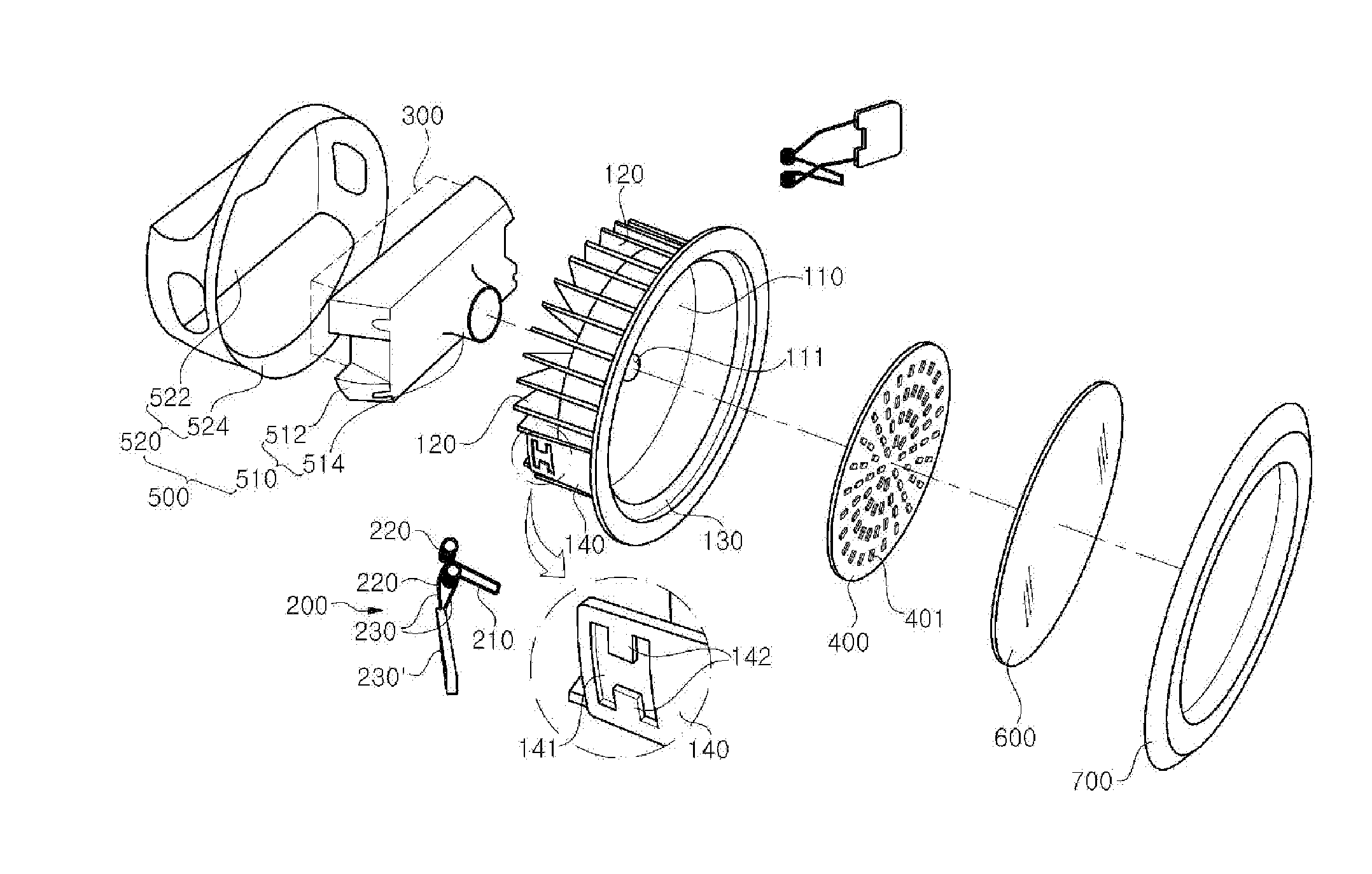
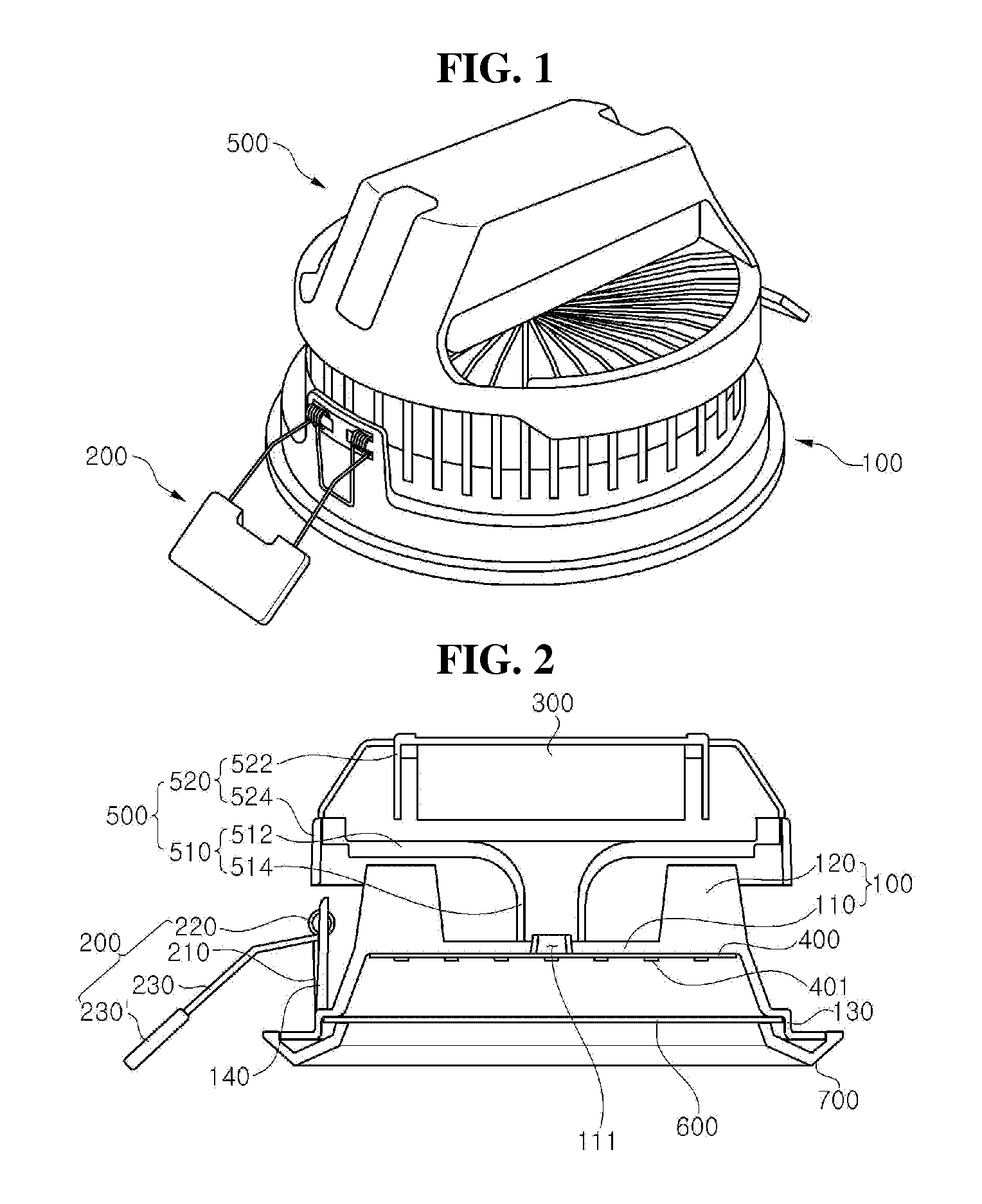
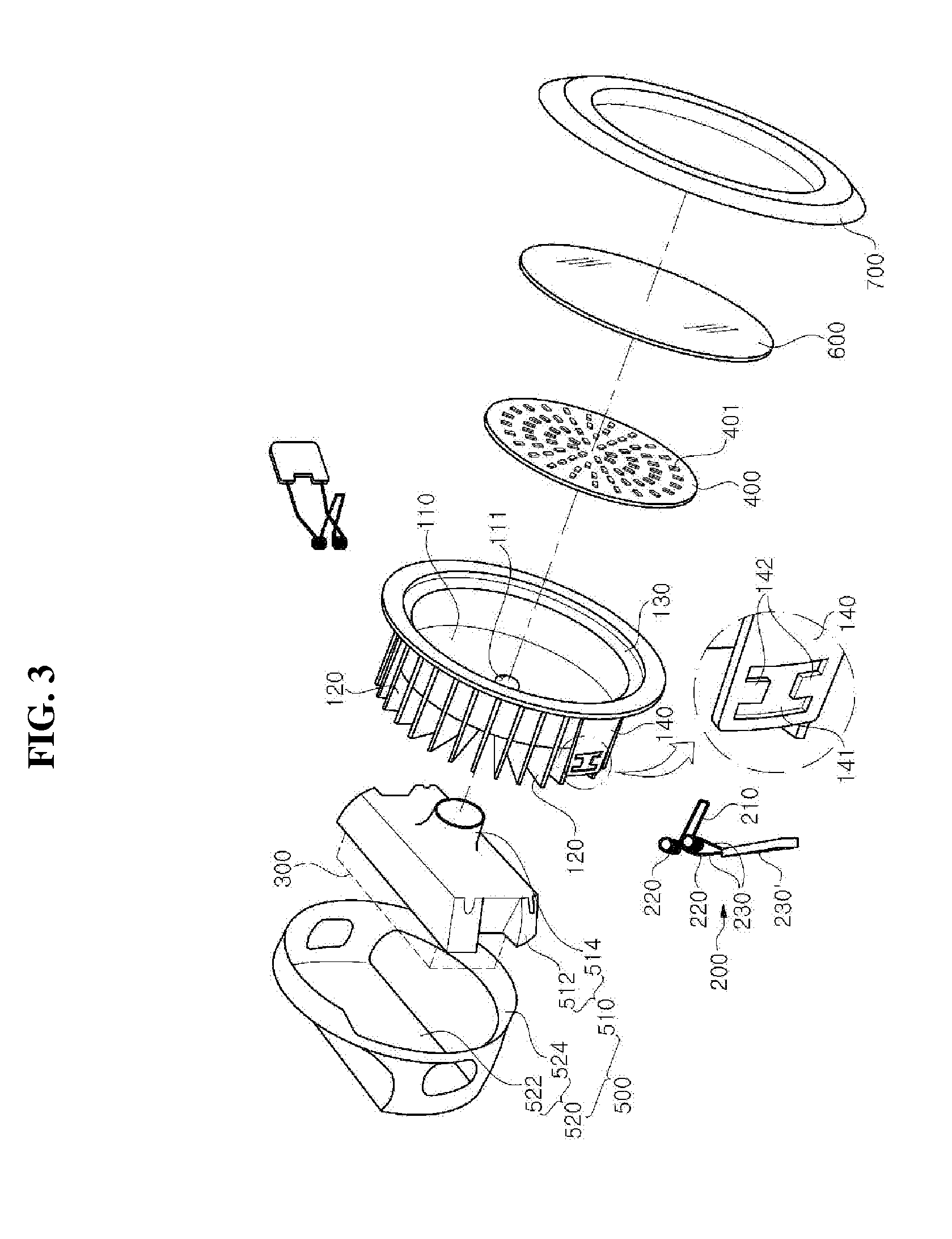
[0037]FIG. 1 is a perspective view showing the entire configuration of an optical semiconductor illuminating apparatus according to an exemplary embodiment of the present invention; FIG. 2 is a cut-away cross-sectional perspective view showing the entire structure of an inner portion of the optical semiconductor illuminating apparatus according to the exemplary embodiment of the present invention; and FIG. 3 is an exploded perspective view showing the entire configuration of the optical semiconductor illuminating apparatus according to the exemplary embodiment of the present invention.

[0038]It may be appreciated that the optical semiconductor illuminating apparatus according to the exemplary embodiment of the present invention has a configuration in which a bracket assembly 500 having a power supply 300 embedded therein is mounted at an upper side of a heat...


PUM


Abstract

An optical semiconductor illuminating apparatus capable of being simply installed and built, easily detecting a fault generation point, being simply repaired and replaced, and being compactly implemented. A bracket assembly having a power supply embedded therein is mounted at an upper side of a heat sink including a fixed unit, the power supply is seated on the heat sink including the fixed unit, a plurality of heat radiation fins protrude from an inner surface of the heat sink, and an upper surface of the power supply is disposed at a position higher than or equal to that of an edge of an upper end portion of the heat sink.

Description

CROSS-REFERENCE TO RELATED APPLICATION[0001]This application claims priority from and the benefit of Korean Patent Application No. 10-2011-0147879, filed on Dec. 30, 2011, and No. 10-2011-0147880, filed on Dec. 30, 2011, which is hereby incorporated by reference for all purposes as if fully set forth herein.BACKGROUND OF THE INVENTION[0002]1. Field of the Invention[0003]The present invention relates to an optical semiconductor based illuminating apparatus.[0004]2. Discussion of the Background[0005]An optical semiconductor such as a light emitting diode (LED) or a laser diode (LD) is one of the components that have been recently spotlighted widely as an illuminating apparatus due to lower power consumption, a longer lifespan, more excellent durability, and significantly higher brightness as compared with an incandescent lamp and a fluorescent lamp.[0006]Recently, the optical semiconductor has tended to be utilized for downlight illumination.[0007]In the downlight mainly having a form...

Claims


Application Information

Patent Timeline
IPC IPC(8): F21V29/00F21S8/00
CPCF21V21/044F21V23/023F21Y2101/02F21Y2105/001F21V29/773F21V17/10F21V29/2212F21Y2101/025F21S8/026F21Y2105/10F21Y2115/10
Inventor SONG, TAE HOONKIM, JI WAN
Owner POSCO LED
Why Eureka
Try Eureka