Circuit device and inkjet head assembly

Active Publication Date: 2013-12-26
FUJIFILM CORP
View PDF8 Cites 0 Cited by
  • Summary
  • Abstract
  • Description
  • Claims
  • Application Information

AI Technical Summary

Benefits of technology

[0014]According to the present invention, the dried body is brought into contact with the end portion of the circuit board while movement of the dried body is guided by the guiding member. This makes it possible to pre

Problems solved by technology

However, while the circuit device described in Japanese Patent Application Laid-Open No. 2010-86992 can prevent the short circuit of the conductive patterns which may occur due to an intrusion of water from the board surface (semiconductor element mounting surfac

Method used


Image

  • Circuit device and inkjet head assembly
  • Circuit device and inkjet head assembly
  • Circuit device and inkjet head assembly

Examples


Example

EXAMPLE

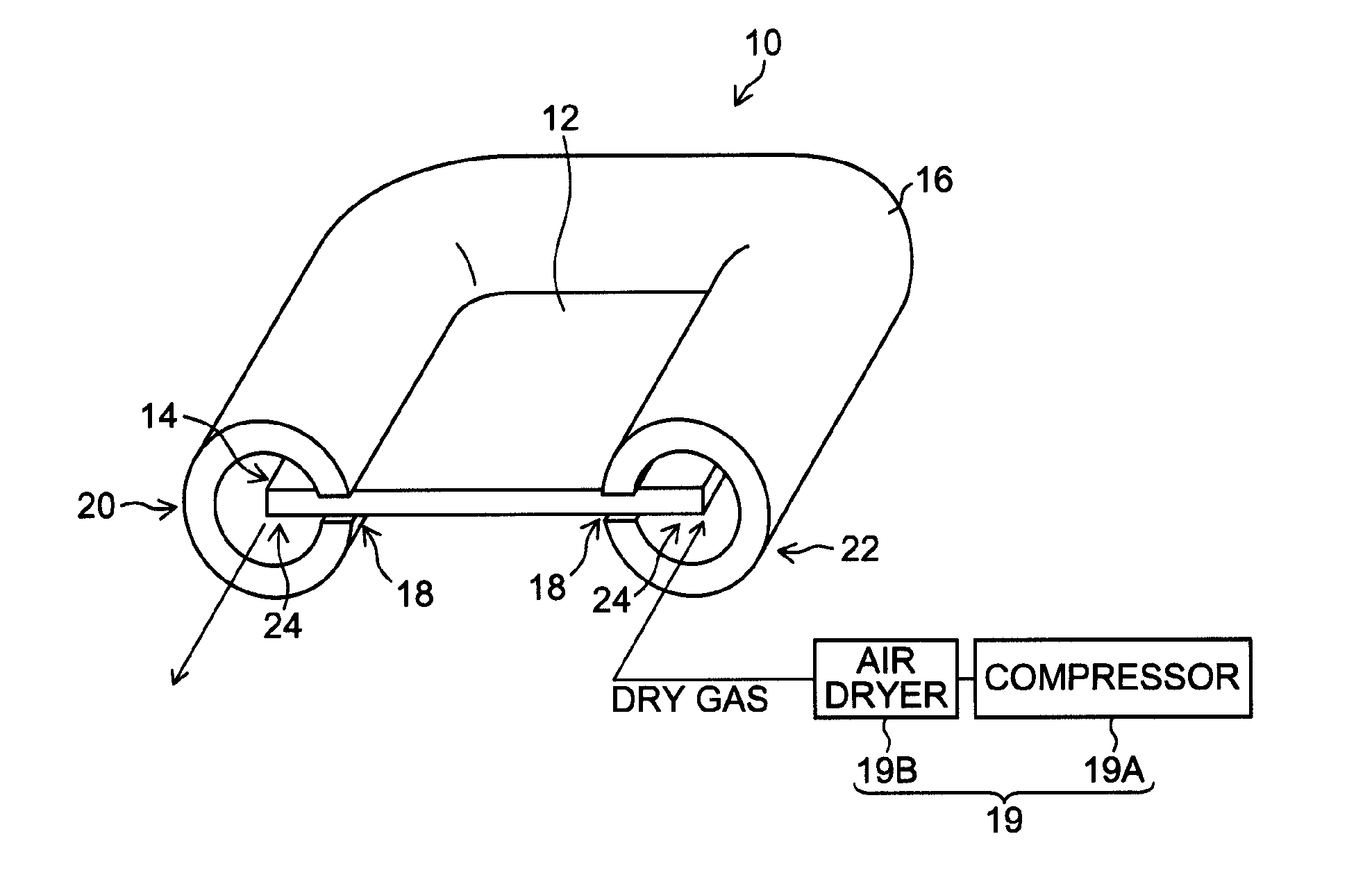
[0055]As the guiding member 16 (see FIG. 1), a tube made of polyvinyl chloride (PVC) (10 millimeters in diameter) is applied. A part of a peripheral portion of the tube is cut open along a central axis to form a notch portion (shown in FIG. 1 with reference numeral 18).

[0056]Respective sides of the circuit board 12 (see FIG. 1) are inserted into the notch portion 18, so that all the end faces of the circuit board 12 are coated with the guiding member 16 (see FIG. 6).

[0057]A contact interface between the surface (surface having the wiring layer 32 formed thereon and being covered with the insulating layer 34) of the circuit board 12 and the guiding member 16, and a contact interface between the back surface of the circuit board 12 and the guiding member 16 are sealed with adhesives provided thereto.

[0058]The circuit board 12 with the guiding member 16 mounted thereon is put in an unshown constant temperature / constant humidity chamber (85° C., 85% (RH)) and a direct voltage of ...

Example

COMPARATIVE EXAMPLE 1

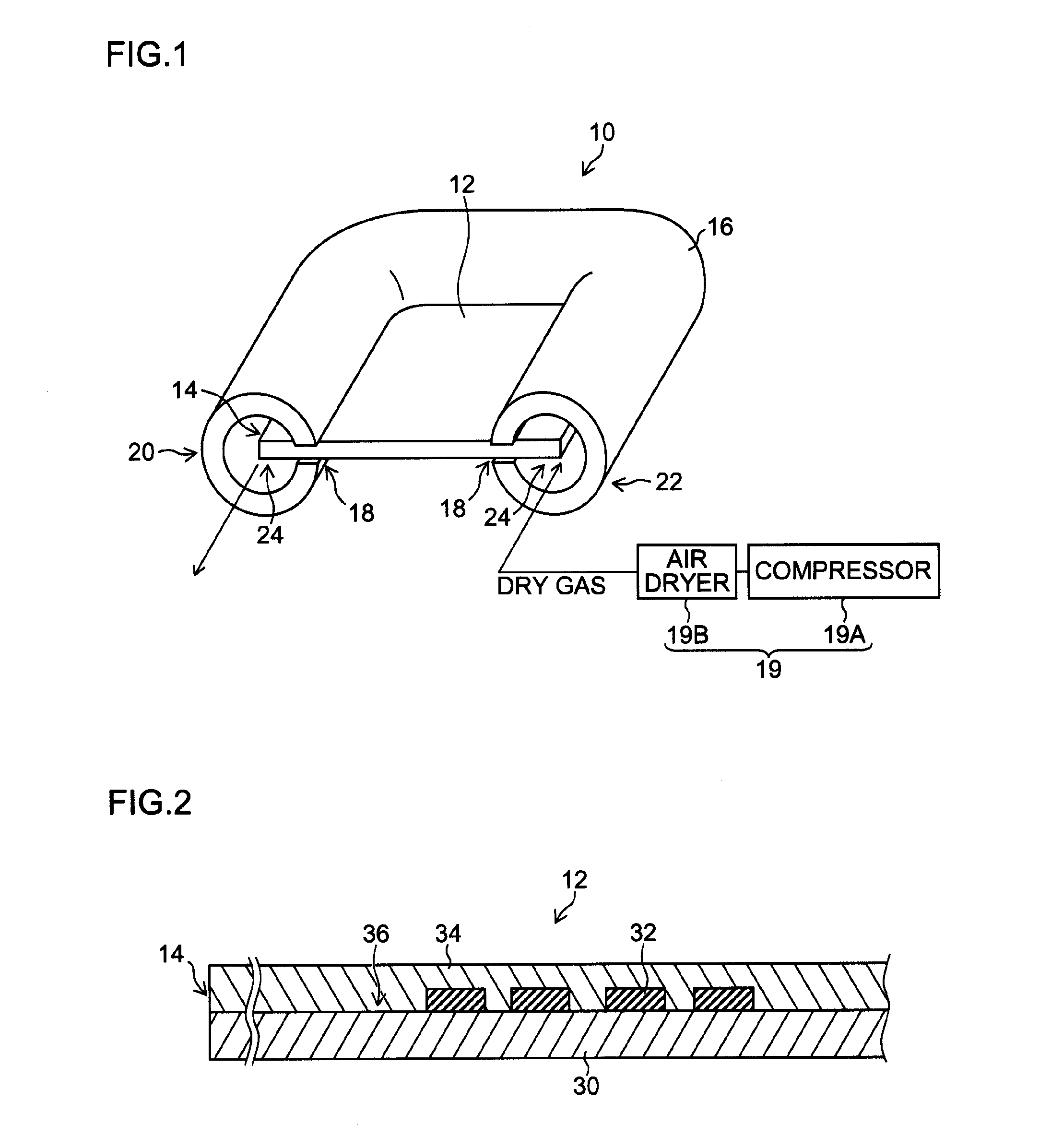
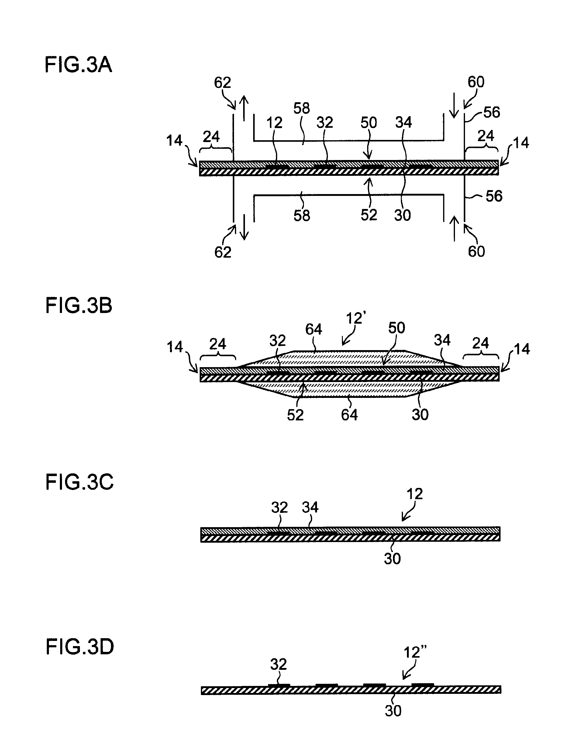
[0059]As in the example described in the foregoing, the circuit board 12 shown in FIG. 2 is used as a printed-circuit board.

[0060]As shown in FIG. 3A, a sealing member 56 is mounted on a part other than the peripheral portion 24 so as to remain the peripheral portion 24 (in the vicinity of the end face 14) of a surface 50 and a back surface 52 of the circuit board 12.

[0061]The sealing member 56 has a space portion 58 formed in the inside and has flow channel portions 60 and 62 formed so as to communicate with the space portion 58.

[0062]The circuit board 12 with the sealing member 56 mounted thereon is put in the constant temperature / constant humidity chamber (85° C., 85% (RH)) under the environment conditions set same as those in the example, and a direct voltage of 12 volts is applied to the wiring layer 32. Dry gas (85° C., 25% (RH)) is supplied to the inside of the sealing member 56 and is circulated therein so that a constant temperature / constant humidity en...

Example

Comparative Example 2

[0064]As shown in FIG. 3B, a circuit board 12′ is applied in the comparative example 2, in which a section other than the peripheral portion 24 of the surface 50 and the back surface 52 of the circuit board 12 shown in FIG. 2 is coated with water glass 64.

[0065]The circuit board 12′ which is coated with the water glass 64 except the peripheral portion 24 is put in the constant temperature / constant humidity chamber (85° C., 85% (RH)) under the environment conditions set same as those in the example, and a direct voltage of 12 volts is applied to the wiring layer 32.


PUM


Abstract

A circuit device according to an aspect of the present invention includes a circuit board which has one or more wiring layers formed on a base material and has an insulating layer laminated on a surface of the base material opposite to the one or more wiring layers, and a guiding member which is configured to encircle at least a part of an end face of the circuit board so that a space is formed with the end face and to guide movement of a dried body which is supplied to the formed space.

Description

BACKGROUND OF THE INVENTION[0001]1. Field of the Invention[0002]The present invention relates to a circuit device and an inkjet head assembly, and more particularly relates to a technology for protecting an electrical wiring pattern on a circuit board.[0003]2. Description of the Related Art[0004]There is known a circuit board configured to include a base material, such as a resin film and glass epoxy, a thin film made of a metallic material, such as copper, formed on the base material, an electrical wiring pattern formed by patterning the metal film by etching or other methods, and further a coating made of an insulating material, such as a solder resist, for coating the electrical wiring pattern.[0005]The circuit board is widely used in industrial equipment and / or consumer equipment. Thus, as the circuit board is used in various applications and environments, the use environments of the circuit board are assumed to include a high-humidity environment, a high-temperature environment...

Claims


Application Information

Patent Timeline
IPC IPC(8): H05K10/00B41J2/01
CPCH05K10/00B41J2/01B41J2/14233B41J2002/14362B41J2002/14491B41J2202/12
Inventor ONODERA, DAISUKEWAKABAYASHI, AKIRA
Owner FUJIFILM CORP
Why Eureka
Try Eureka