Check patentability & draft patents in minutes with Patsnap Eureka AI!

Display unit

a display unit and display technology, applied in the field of display units, can solve problems such as image quality reduction, and achieve the effects of reducing the lowering of image quality caused by diffraction reflection, and reducing the generation of diffraction reflection in a certain direction

Active Publication Date: 2014-01-30
SONY CORP
View PDF5 Cites 1 Cited by
  • Summary
  • Abstract
  • Description
  • Claims
  • Application Information

AI Technical Summary

Benefits of technology

The patent describes a display device which prevents the reduction of image quality caused by outside light. This is achieved by shaping the sources and drain region of the transistors in the device in a way that reduces diffraction reflection. This results in a more optimal image quality for the display device.

Problems solved by technology

Accordingly, there is a disadvantage that the reflected light is viewed by an observer (not illustrated), and image quality is lowered.

Method used


Image

  • Display unit
  • Display unit
  • Display unit

Examples


first embodiment (

1. First embodiment (source area is large)

2. Modified example

second embodiment (

3. Second embodiment (including a continuous curved face in an end of a cathode)

4. Modified example

5. Module and application examples

1. First Embodiment

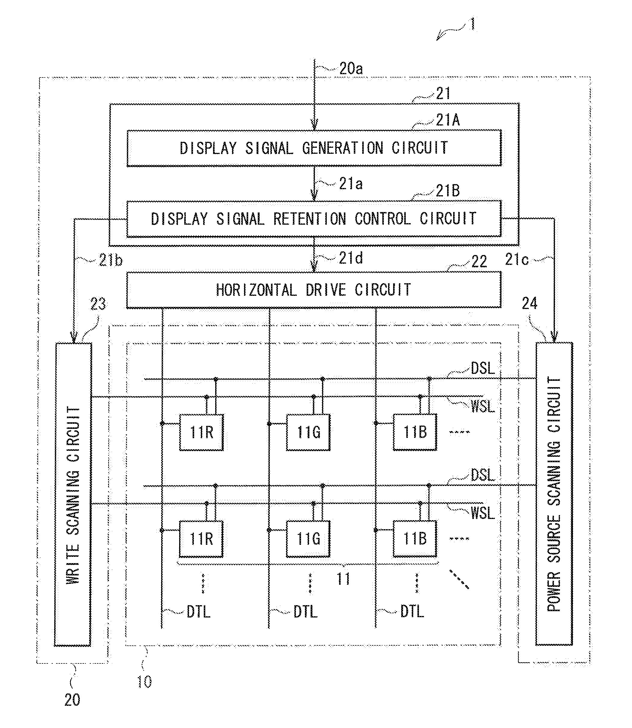
[0041]FIG. 1 illustrates an example of a whole configuration of a display unit 1 according to a first embodiment of the invention. The display unit 1 includes a display section 10 and a peripheral circuit section 20 (drive section) formed on the periphery of the display section 10 on a substrate 40 (described later) made of, for example, glass, a silicon (Si) wafer, a resin or the like.

Display Section 10

[0042]In the display section 10, a plurality of pixels 11 are arranged in a matrix state over the whole area of the display section 10. The display section 10 displays an image based on a video signal 20a inputted from outside by active matrix drive. Each pixel 11 includes a red-use pixel 11R, a green-use pixel 11G, and a blue-use pixel 11B.

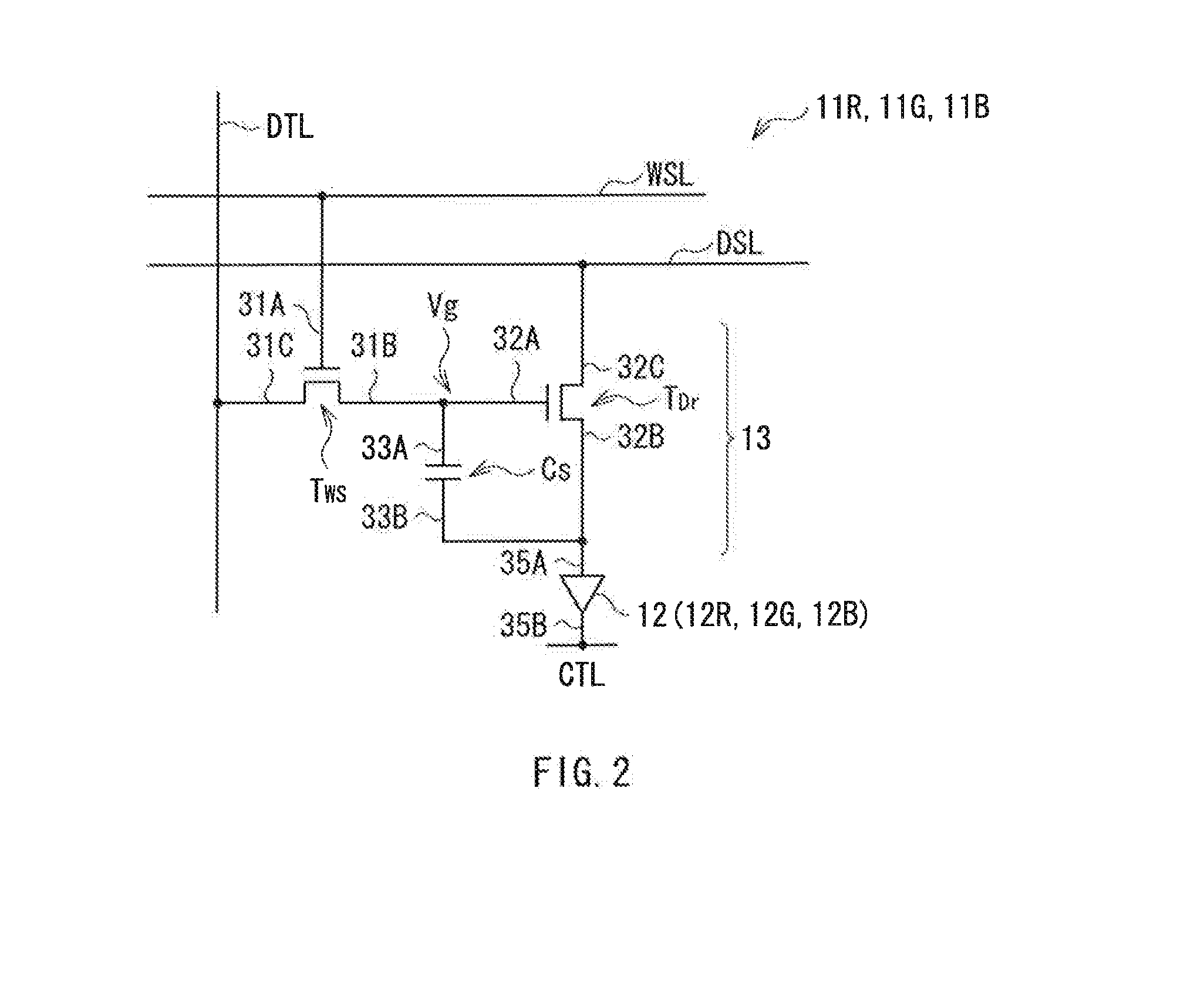
[0043]FIG. 2 illustrates an example of a circuit configuration of the pixels 11R, 11G, and 11B....

second embodiment

[0064]FIG. 6 illustrates a layout of the pixel 11 (11R, 11G, and 11B) of a display unit according to a second embodiment of the invention. The configuration of the display unit of this embodiment is different from the configuration of the display unit 1 of the foregoing embodiment and the modified example thereof in that agate 52A is included instead of the gate 32A of the transistor TDr and a source 52B is included instead of the source 32B of the transistor TDr. Further, the configuration of the display unit of this embodiment is different from the configuration of the display unit 1 of the foregoing embodiment and the modified example thereof in that a terminal 53A is included instead of the terminal 33A of the retentive capacity Cs, and a terminal 53B is included instead of the terminal 33B of the retentive capacity Cs, respectively. Thus, a description will be hereinafter mainly given of different points from the foregoing embodiment and the modified example thereof, and a desc...


PUM


Abstract

A display unit with which diffraction reflection is able to be decreased is provided. The display unit includes a display section having an organic EL device and a pixel circuit for every pixel. The pixel circuit has a first transistor for writing a video signal and a second transistor for driving the organic EL device based on the video signal written by the first transistor. The second transistor has a gate, a source and a drain. The organic EL device has an anode, an organic layer, and a cathode. An upper face of the source or the drain is formed at least in a region opposed to the anode or the cathode.

Description

CROSS-REFERENCE TO RELATED APPLICATION[0001]The present application is a continuation of U.S. patent application Ser. No. 12 / 660,319, filed on Feb. 24, 2010, which claims priority from Japanese Patent Application No. JP 2009-053159 filed in the Japanese Patent Office on Mar. 6, 2009, all of which are incorporated herein by reference.BACKGROUND OF THE INVENTION[0002]1. Field of the Invention[0003]The present invention relates to a display unit including an organic EL (electro luminescence) device.[0004]2. Description of the Related Art[0005]In recent years, in the field of display units for displaying images, display units including as a light emitting device of a pixel, a current drive type optical device with the emission luminance changeable according to the flowing current value such as an organic EL device have been developed, and such display units are facilitated to be commercialized (for example, see Japanese Unexamined Patent Application Publication No. 2008-083272).[0006]Th...

Claims


Application Information

Patent Timeline
Patent Type & Authority Applications(United States)
IPC IPC(8): G09G3/30
CPCG09G3/30G09G3/3233G09G3/3291H10K59/1213H10K2102/3026H10K59/805H10K59/12H10K59/8791H10K59/35H10K50/86H10K50/805
Inventor TANEDA, TAKAYUKIYAMAMOTO, TETSUROUCHINO, KATSUHIDESEO, YUKI
Owner SONY CORP
Features
  • R&D
  • Intellectual Property
  • Life Sciences
  • Materials
  • Tech Scout
  • Unparalleled Data Quality
  • Higher Quality Content
  • 60% Fewer Hallucinations
Learn More