Supercharge Your Innovation With Domain-Expert AI Agents!

System and method for analyzing electronic devices having opposing thermal components

Inactive Publication Date: 2014-03-27
EXATRON
View PDF3 Cites 0 Cited by
  • Summary
  • Abstract
  • Description
  • Claims
  • Application Information

AI Technical Summary

Benefits of technology

The invention is a system for analyzing electronic devices by using a transport apparatus to move the devices from an input station to an electric machine interface station. The system includes an electric machine interface that engages with each device and simultaneously transfers heat or cooling to the device using a thermal component. The system also includes a support structure and a temperature modification device that can modify the temperature of the fluid before it flows through the system. The system can also include a communications interface and an electric machine actuator to move the electric machine interface into and out of contact with the communications interface. The technical effects of the invention include improved analysis of electronic devices and efficient modification of their temperature.

Problems solved by technology

Alignment between contacts of the electronic device and the terminals of the electric machine interface is always difficult to achieve.
Such a temperature profile makes it difficult to determine accurate measurements for the electronic device as it would perform under conditions where the temperature through the electronic device is uniform, for example under all steady state conditions.
Because of requirements for throughput, it is not practical to wait for every device to achieve steady state temperature conditions.
A thermocouple is usually used for purposes of measuring temperature in a vicinity of the electronic device, but it is not possible to obtain the exact temperature of the electronic device at any particular moment in time using a thermal couples because of differences in temperature at the thermal couple and at the electronic device.

Method used


Image

  • System and method for analyzing electronic devices having opposing thermal components
  • System and method for analyzing electronic devices having opposing thermal components
  • System and method for analyzing electronic devices having opposing thermal components

Examples


Embodiment Construction

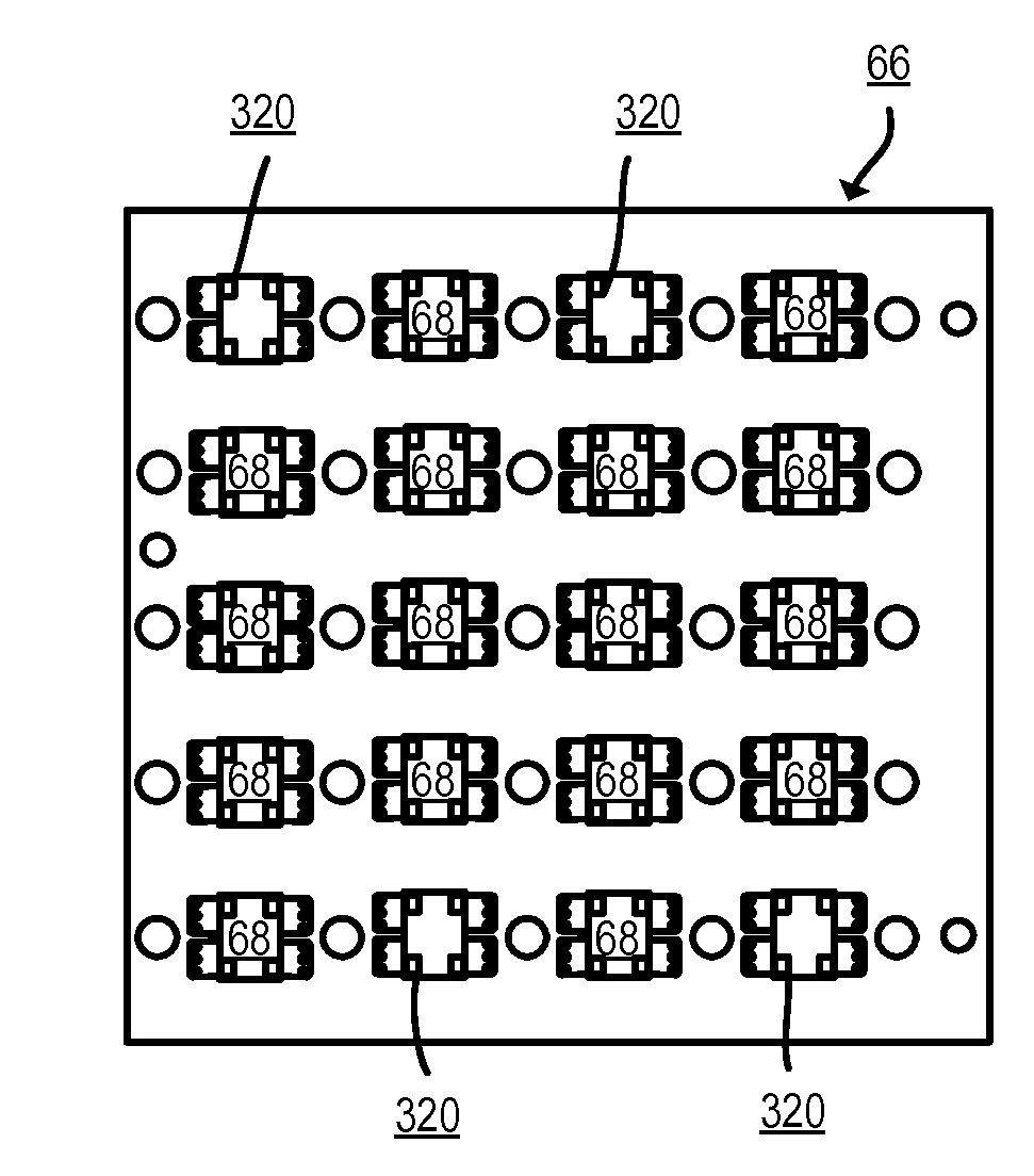
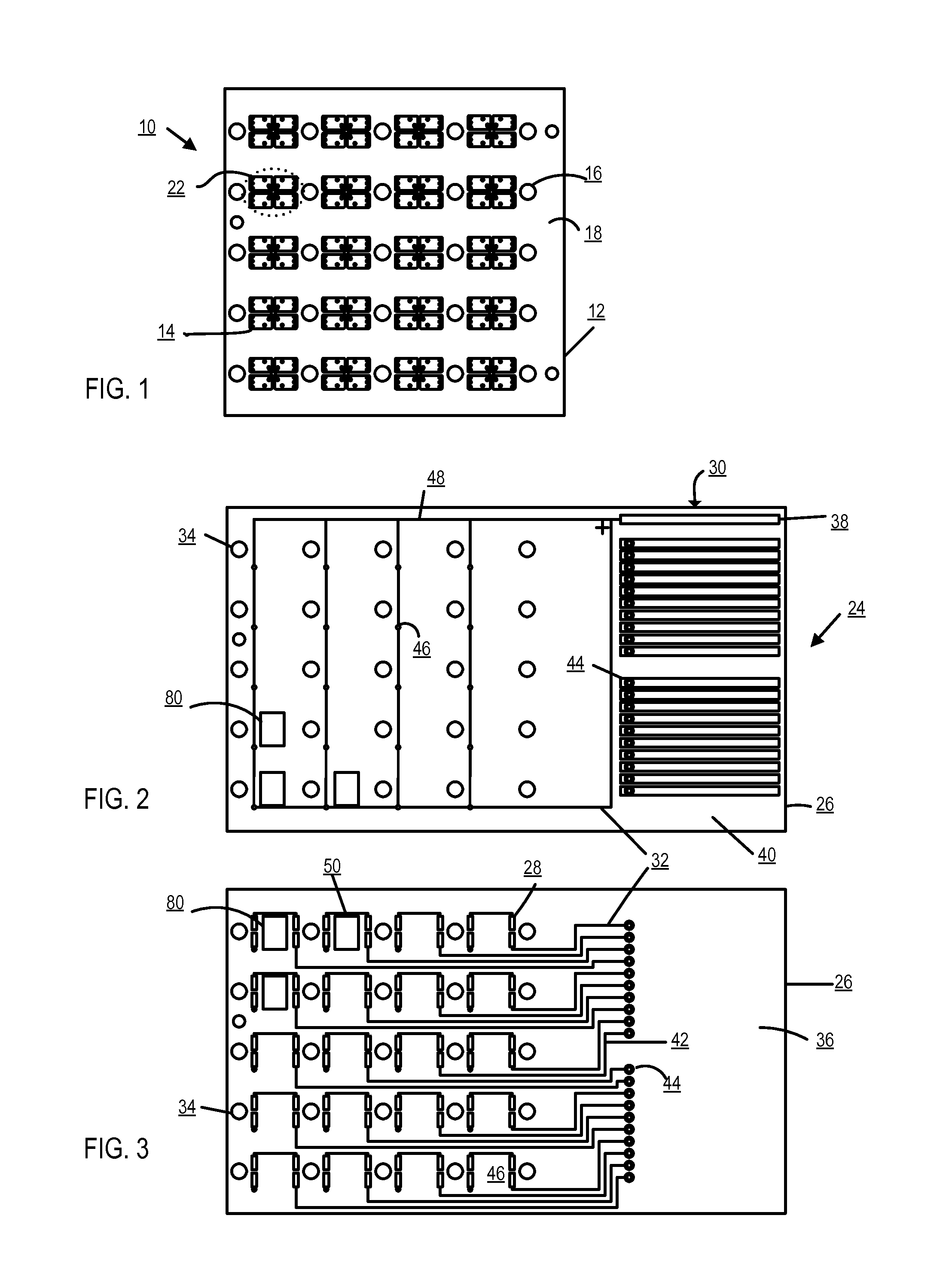
[0047]FIG. 1 of the accompanying drawings illustrates an interposer 10 having a substrate 12 and terminals 14. The substrate 12 is made of a thin non-conductive material. Fastener alignment openings 16 are formed through the interposer 10.

[0048]The terminals 14 are formed on an upper surface 18 of the substrate 12. The terminals 14 are formed in sets 22 of four terminals 14. In another embodiment there may be six or more of the terminals 14 in different layouts. The sets 22 are arranged in four columns and five rows for a total of 20 of the sets 22. Other layouts may be possible without departing from the scope of the invention. No terminals are formed on a lower surface of the substrate 12 and no conductive vias are formed through the substrate 12.

[0049]FIGS. 2 and 3 illustrate a printed circuit board 24 that includes a substrate 26, terminals 28, a communications interface 30 and leads 32.

[0050]The substrate 26 is made of a non-conductive material. Fastener alignment openings 34 a...


PUM


Abstract

A system for analyzing electronic devices includes an input station, a transport apparatus, an electric machine interface station, an electric machine interface, a support structure and first and second thermal components. The input station receives a plurality of electronic devices and the transport apparatus transports each of the electronic devices from the input station to the electric machine interface station. The electric machine interface engages the electronic device when the electronic device is at the electric machine interface station, and is disengageable from the electronic device for the electronic device to be transportable by the transport apparatus away from the electric machine interface station. The first and second thermal components are located on opposing sides of the electronic device when the electronic device is at the electric machine interface station to simultaneously transfer heat to or from the electronic device.

Description

BACKGROUND OF THE INVENTION[0001]1. Field of the Invention[0002]This invention relates generally to a system and method for analyzing electronic devices, including determining a parameter of a measured electronic device.[0003]2. Discussion of Related Art[0004]Before electronic devices are packaged for shipping, it is often required to measure certain parameters of the electronic devices. The parameters may for example be used for programming the electronic devices or may be measured to determine correct functioning of the electronic devices.[0005]A system that is used for analyzing electronic devices often includes a handler and an electric machine. The handler may for example have a bin where electronic devices are loosely deposited, a feed mechanism that feeds the devices one at a time and an electric machine interface station where one electronic device at a time is located against terminals of an electric machine interface. The electric machine is connected to the electric machi...

Claims


Application Information

Patent Timeline
IPC IPC(8): G01R31/02
CPCG01R31/2867G01R31/2874G01R31/2893
Inventor HOWELL, ROBERT P.
Owner EXATRON
Features
  • R&D
  • Intellectual Property
  • Life Sciences
  • Materials
  • Tech Scout
  • Unparalleled Data Quality
  • Higher Quality Content
  • 60% Fewer Hallucinations
Learn More