Stiction-free drying process with contaminant removal for high-aspect ratio semiconductor device structures

a semiconductor device, high-aspect ratio technology, applied in the direction of cleaning process and apparatus, cleaning process using liquids, chemistry apparatus and processes, etc., can solve the problems of high difficulty in drying substrates with high aspect ratio features or low-k materials with voids or pores, and workable drying practices are facing a steep rise in difficulty, so as to reduce or eliminate the negative effect of line stiction

Active Publication Date: 2014-05-29
APPLIED MATERIALS INC
View PDF8 Cites 64 Cited by
  • Summary
  • Abstract
  • Description
  • Claims
  • Application Information

AI Technical Summary

Benefits of technology

[0008]Embodiments provided herein generally relates to a method of cleaning a substrate and a substrate processing apparatus. More specifically, embodiments relate to a method of cleaning a substrate in a manner that reduces or eliminates the negative effects of line stiction between semiconductor device features. Other embodiments relate to a substrate processing apparatus that allows for cleaning of the substrate in a manner that reduces or eliminates line stiction between semiconductor device features.

Problems solved by technology

Drying of the substrate that has high aspect ratio features or low-k materials which have voids or pores is very challenging subsequent to the application of a cleaning liquid.
Capillary forces of the cleaning liquid often cause deformation of materials in these structures which can create undesired stiction, which can damage the semiconductor substrate in addition to leaving residue on the substrate from the cleaning solution utilized.
The aforementioned drawbacks are especially apparent on substrates with high-aspect-ratio semiconductor device structures during subsequent drying of the substrate.
Current workable drying practices are facing a steeply rising challenge in preventing line stiction as a result of rapid device scaling advancements.

Method used


Image

  • Stiction-free drying process with contaminant removal for high-aspect ratio semiconductor device structures
  • Stiction-free drying process with contaminant removal for high-aspect ratio semiconductor device structures
  • Stiction-free drying process with contaminant removal for high-aspect ratio semiconductor device structures

Examples


Embodiment Construction

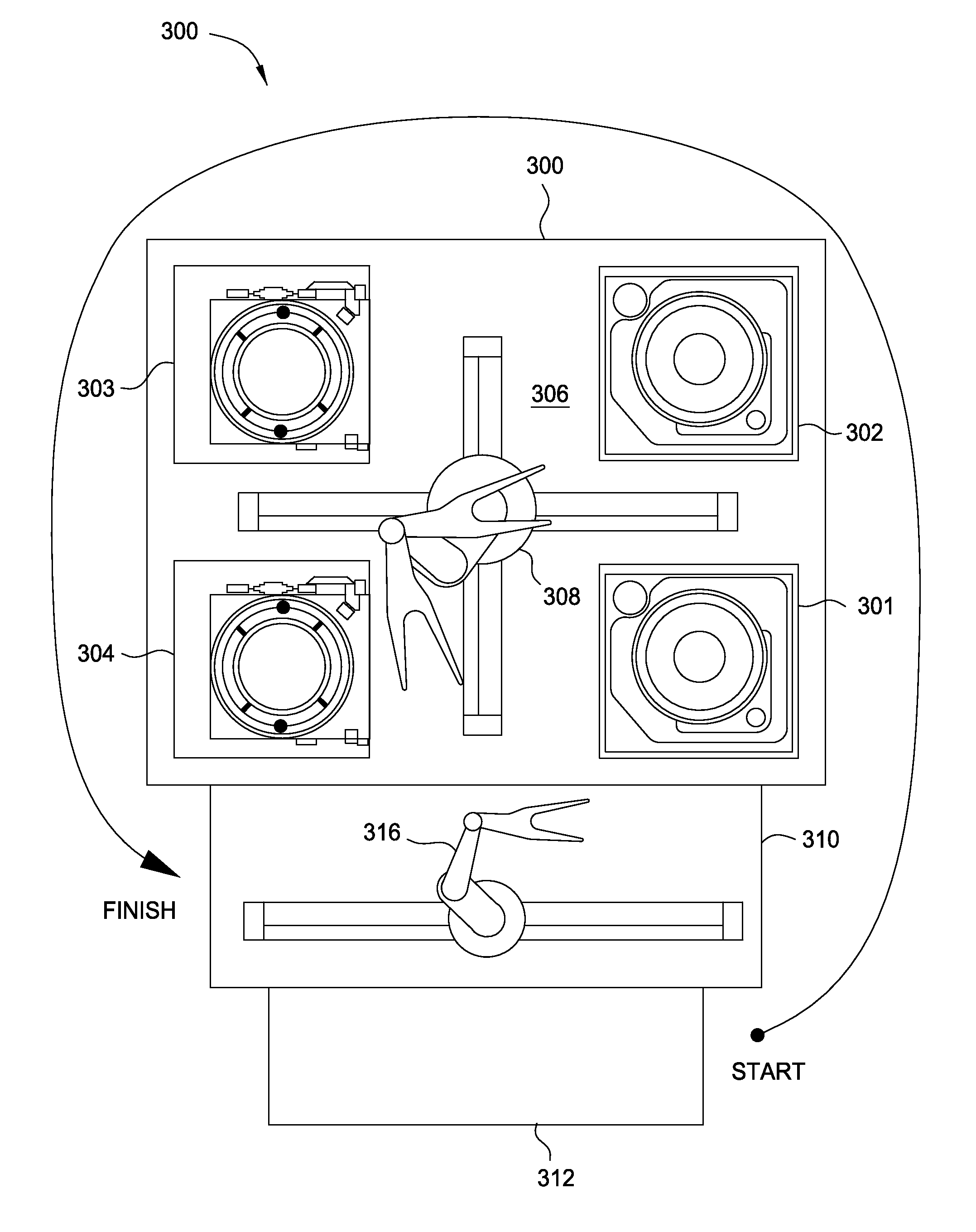
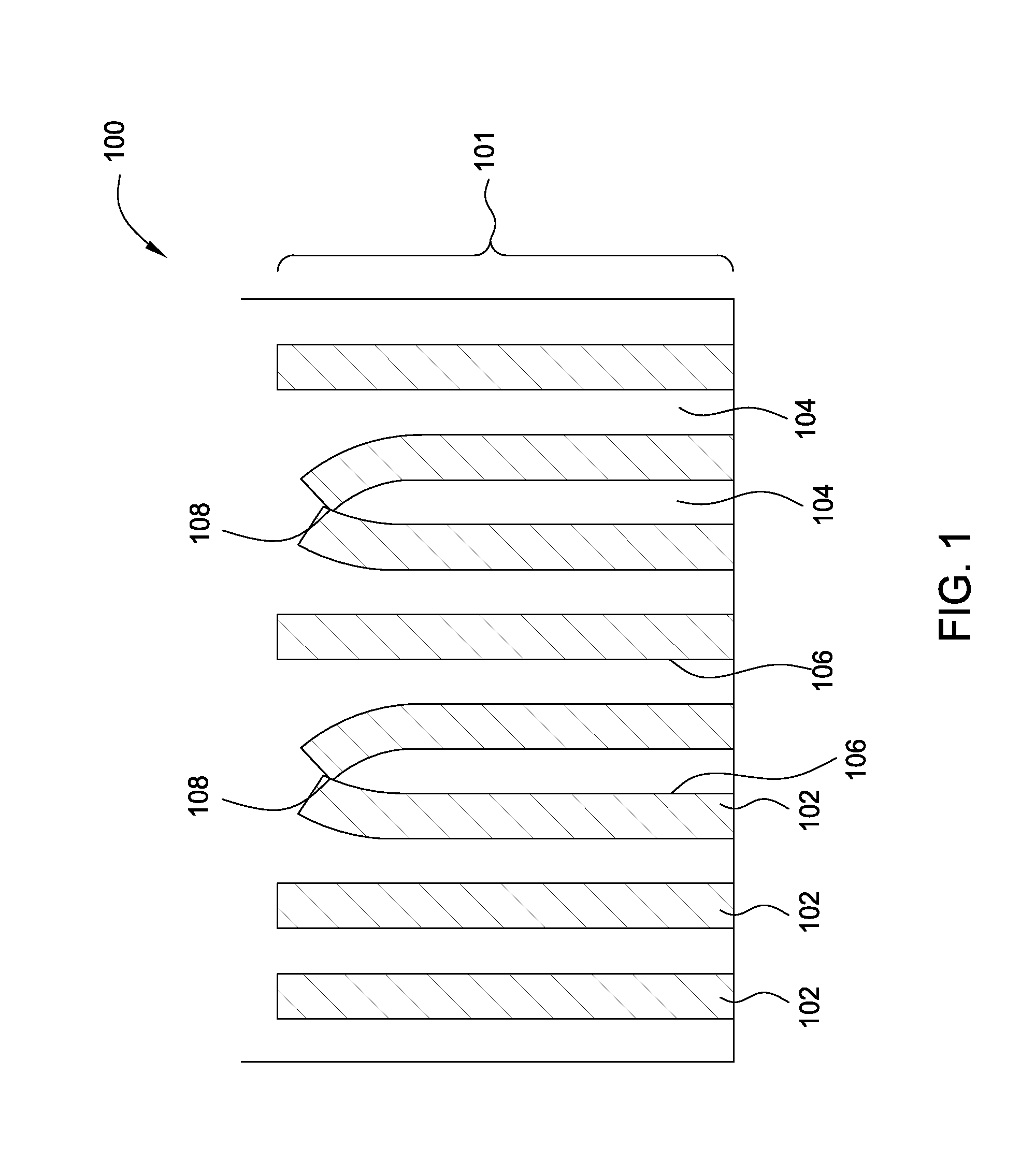
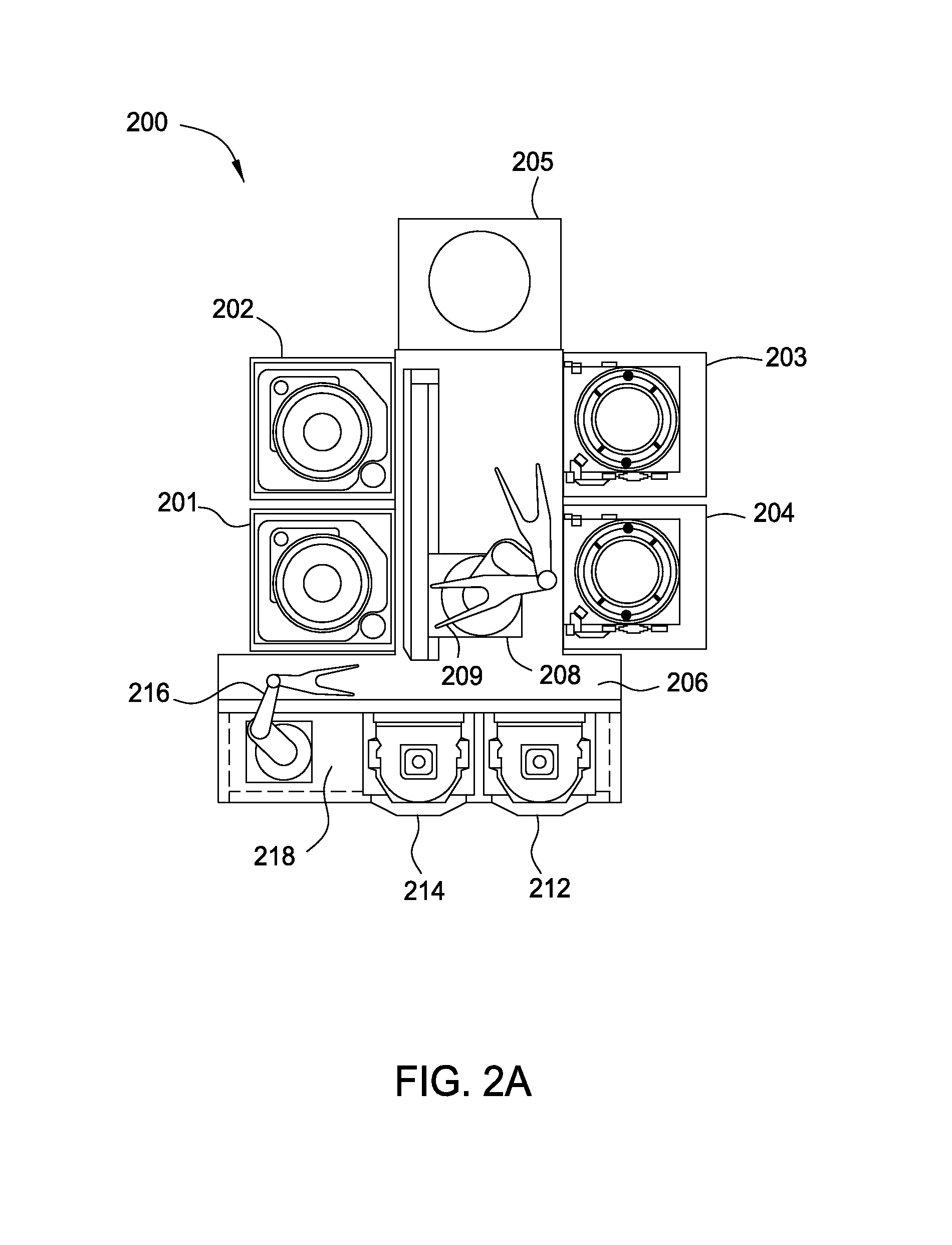
[0029]Embodiments provided herein generally relate to a method and apparatus used to clean a substrate. More specifically, embodiments relate to a method of cleaning a substrate in a manner that reduces or eliminates the line stiction created between semiconductor device features after a wet cleaning process has been performed on the substrate. Other embodiments relate to a substrate processing apparatus that allows for cleaning of the substrate in a manner that reduces or eliminates line stiction between semiconductor device features.

[0030]In the following description, for purposes of explanation, numerous specific details are set forth in order to provide a thorough understanding of the embodiments provided herein. However, it will be evident to one skilled in the art that the present invention may be practiced without these specific details. In other instances, specific apparatus structures have not been described so as not to obscure embodiments described. The following descript...


PUM

PropertyMeasurementUnit
pressureaaaaaaaaaa
wavelengthaaaaaaaaaa

Abstract

Embodiments of the invention generally relate to a method of cleaning a substrate and a substrate processing apparatus that is configured to perform the method of cleaning the substrate. More specifically, embodiments of the present invention relate to a method of cleaning a substrate in a manner that reduces or eliminates the negative effects of line stiction between semiconductor device features. Other embodiments of the present invention relate to a substrate processing apparatus that allows for cleaning of the substrate in a manner that reduces or eliminates line stiction between semiconductor device features formed on the substrate.

Description

CROSS-REFERENCE TO RELATED APPLICATIONS[0001]This application claims benefit of U.S. Provisional Patent Application Ser. No. 61 / 841,779, filed Jul. 1, 2013, and U.S. Provisional Patent Application Ser. No. 61 / 729,965, filed Nov. 26, 2012, which are both herein incorporated by reference.BACKGROUND OF THE INVENTION[0002]1. Field of the Invention[0003]Embodiments of the present invention generally relate to a method and apparatus for cleaning semiconductor substrates, and more specifically, to a stiction-free cleaning and / or drying process for high-aspect-ratio semiconductor device structures.[0004]2. Description of the Related Art[0005]In the cleaning of semiconductor devices, it is necessary to remove liquid and solid contaminants from surfaces of a substrate, thus leaving clean surfaces. Wet cleaning processes generally involve the use of cleaning liquids, such as aqueous cleaning solutions. After wet cleaning the substrate, it is necessary to remove the cleaning liquid from the sur...

Claims


Application Information

Patent Timeline
Patent Type & Authority Applications(United States)
IPC IPC(8): H01L21/02H01L21/67
CPCH01L21/67023H01L21/02041H01L21/02057H01L21/02101H01L21/67034H01L21/67051H01L21/67109H01L21/67126H01L21/67742B08B3/08B08B7/0021
Inventor VERHAVERBEKE, STEVENCHEN, HAN-WENGOUK, ROMAN
Owner APPLIED MATERIALS INC
Why Eureka
Try Eureka