Light emitting device reflective bank structure

a technology of light emitting devices and reflective banks, applied in the direction of semiconductor devices, basic electric elements, electrical equipment, etc., can solve the problem of reducing light extraction efficiency

Active Publication Date: 2014-06-12
APPLE INC
View PDF7 Cites 173 Cited by
  • Summary
  • Abstract
  • Description
  • Claims
  • Application Information

AI Technical Summary

Problems solved by technology

Light emitting from the lateral surfaces of a ...

Method used


Image

  • Light emitting device reflective bank structure
  • Light emitting device reflective bank structure
  • Light emitting device reflective bank structure

Examples


Embodiment Construction

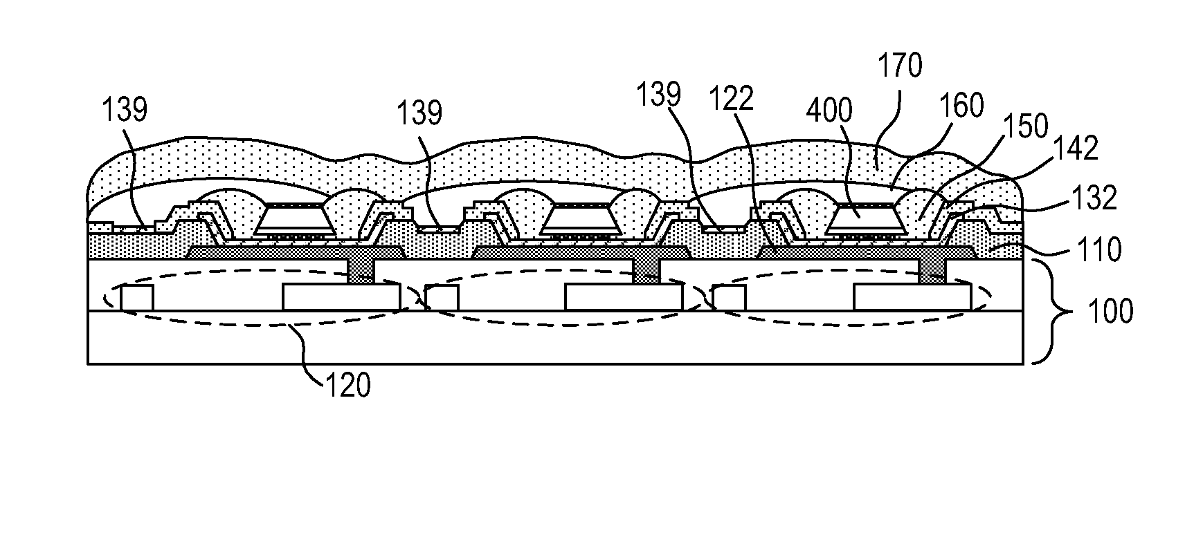
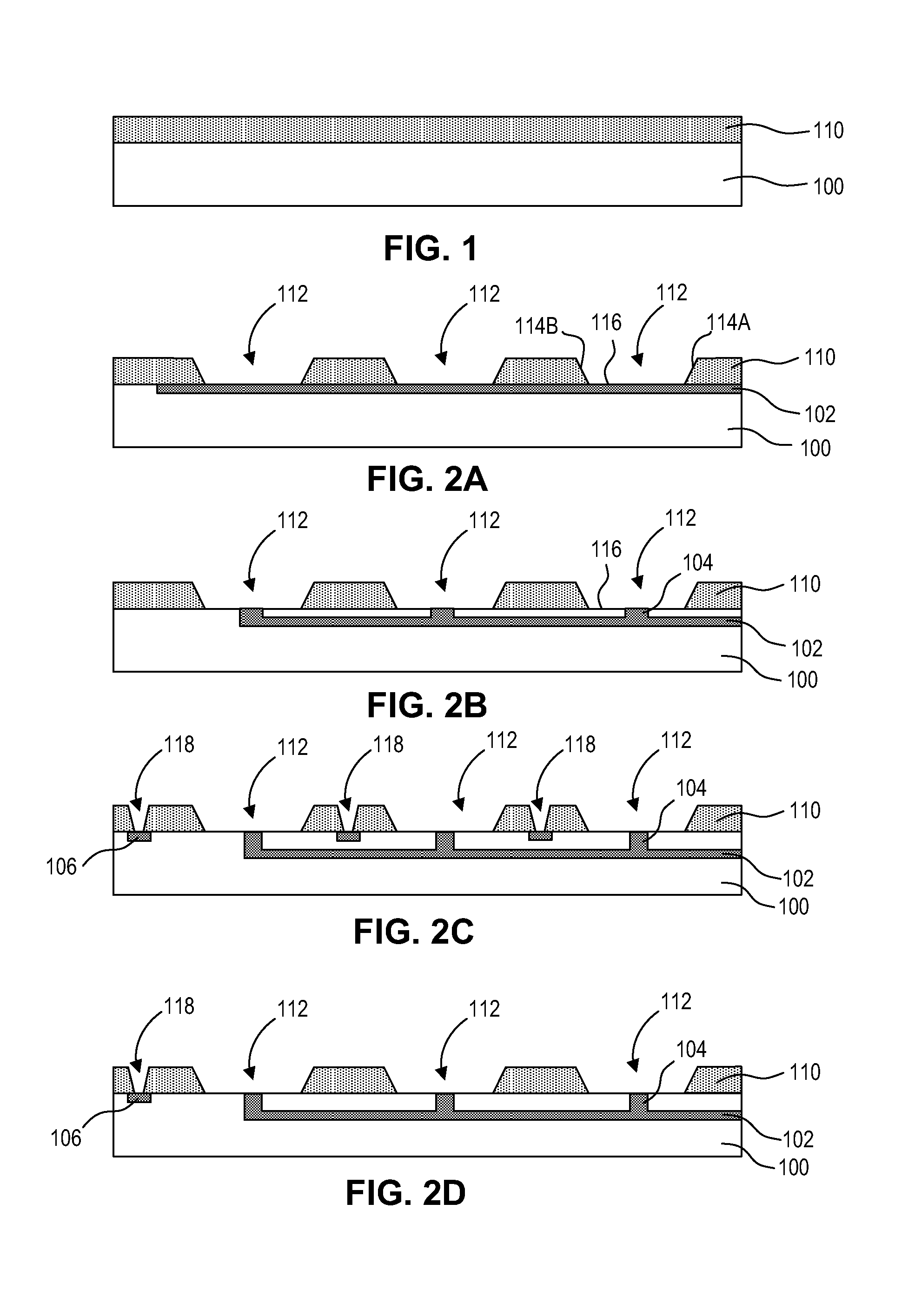
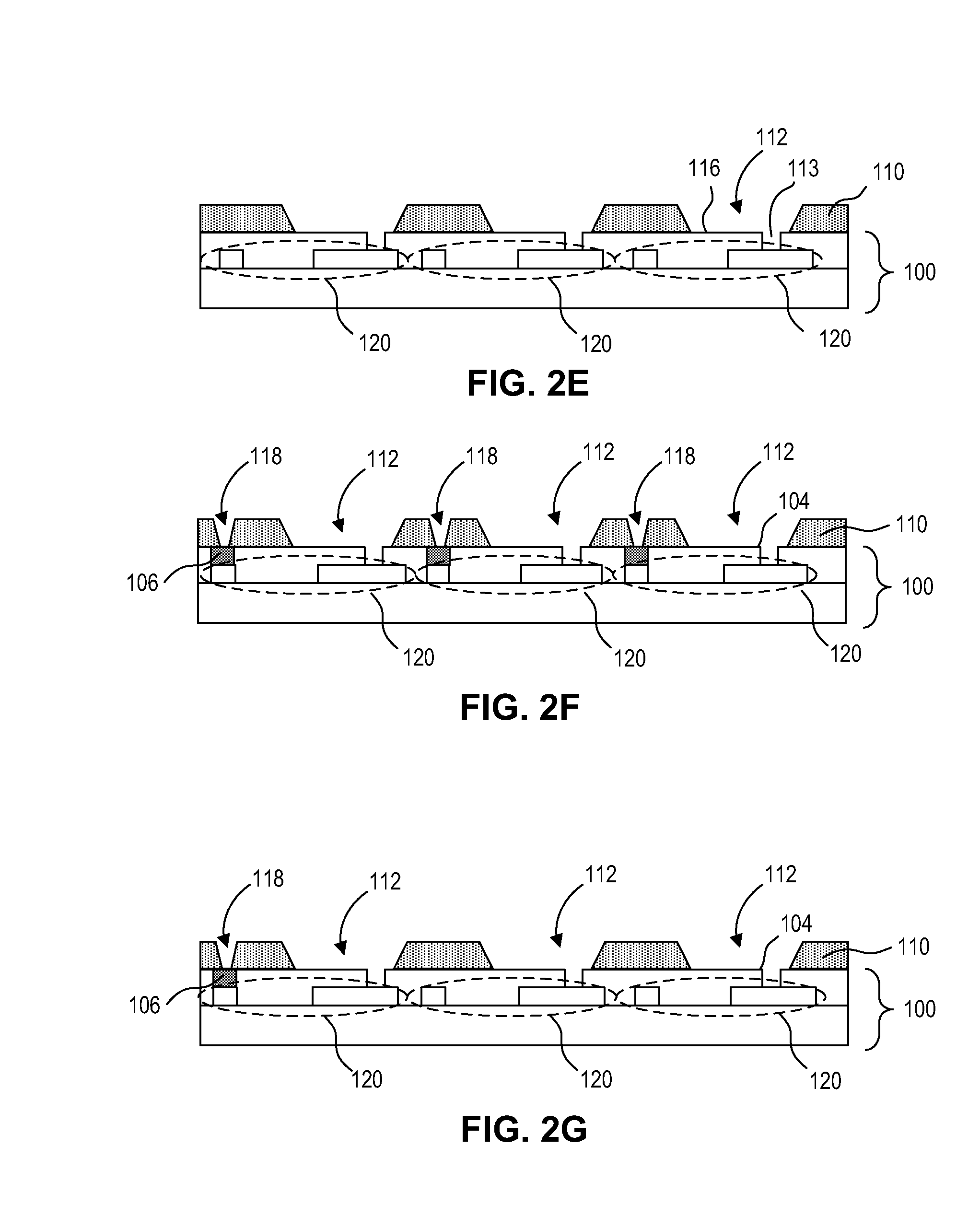
[0102]Embodiments of the present invention describe a reflective bank structure for receiving light emitting devices such as LED devices. For example, the reflective bank structure may be formed on a receiving substrate such as, but not limited to, a display substrate, a lighting substrate, a substrate with functional devices such as transistors or integrated circuits (ICs), or a substrate with metal redistribution lines. While some embodiments of the present invention are described with specific regard to vertical micro LED devices comprising p-n diodes, it is to be appreciated that embodiments of the invention are not so limited and that certain embodiments may also be applicable to other devices which are designed to perform a photonic function (LED, superluminescent diode (SLD), laser).

[0103]The terms “micro” device or “micro” LED structure as used herein may refer to the descriptive size of certain devices or structures in accordance with embodiments of the invention. As used h...


PUM


Abstract

Reflective bank structures for light emitting devices are described. The reflective bank structure may include a substrate, an insulating layer on the substrate, and an array of bank openings in the insulating layer with each bank opening including a bottom surface and sidewalls. A reflective layer spans sidewalls of each of the bank openings in the insulating layer.

Description

BACKGROUND[0001]1. Field[0002]The present invention relates to a reflective bank structure for light emitting devices. More particularly, embodiments of the present invention relate to a reflective bank structure for light emitting diode devices.[0003]2. Background Information[0004]Light emitting diode (LED) devices may include a p-type semiconductor layer, an n-type semiconductor layer, and one or more quantum well layers between the p-type semiconductor layer and the n-type semiconductor layer. The light emitting efficiency of a LED device system depends upon the internal quantum efficiency of the quantum well layer(s) and the light extraction efficiency from the system.[0005]One implementation for increasing light extraction efficiency has been to include a reflective layer in the electrode layer opposite the light emission direction. For example, for a top emission structure, the bottom electrode may include a reflective layer, and vice versa. Light emitting from the lateral sur...

Claims


Application Information

Patent Timeline
IPC IPC(8): H01L27/15
CPCH01L27/15H01L33/48H01L33/60H01L25/0753H01L2224/18H01L2224/83H01L2924/0002H01L2224/95H01L2224/24137H01L2224/73267H01L2224/92244H01L2224/82H10K59/122H01L2924/12041H01L25/167H01L33/44H01L33/62H01L33/06H01L33/36H01L2924/00
Inventor SAKARIYA, KAPIL V.BIBL, ANDREASHU, HSIN-HUA
Owner APPLE INC
Why Eureka
Try Eureka