Check patentability & draft patents in minutes with Patsnap Eureka AI!

Thin film transistor array substrate and organic light-emitting display apparatus including the same

Active Publication Date: 2014-08-28
SAMSUNG DISPLAY CO LTD
View PDF3 Cites 86 Cited by
  • Summary
  • Abstract
  • Description
  • Claims
  • Application Information

AI Technical Summary

Benefits of technology

The present invention provides a way to make thin film transistor arrays and organic light-emitting displays with reduced crosstalk and a more efficient driving voltage line design. This is done by using a mesh structure for the driving voltage lines, which makes them less likely to interfere with each other and to connect to capacitors. Overall, this improves the quality and efficiency of the display.

Problems solved by technology

However, recently, the organic light-emitting display apparatus is required to have high definition, such that available space for the pixel circuit is decreased.

Method used


Image

  • Thin film transistor array substrate and organic light-emitting display apparatus including the same
  • Thin film transistor array substrate and organic light-emitting display apparatus including the same
  • Thin film transistor array substrate and organic light-emitting display apparatus including the same

Examples


Embodiment Construction

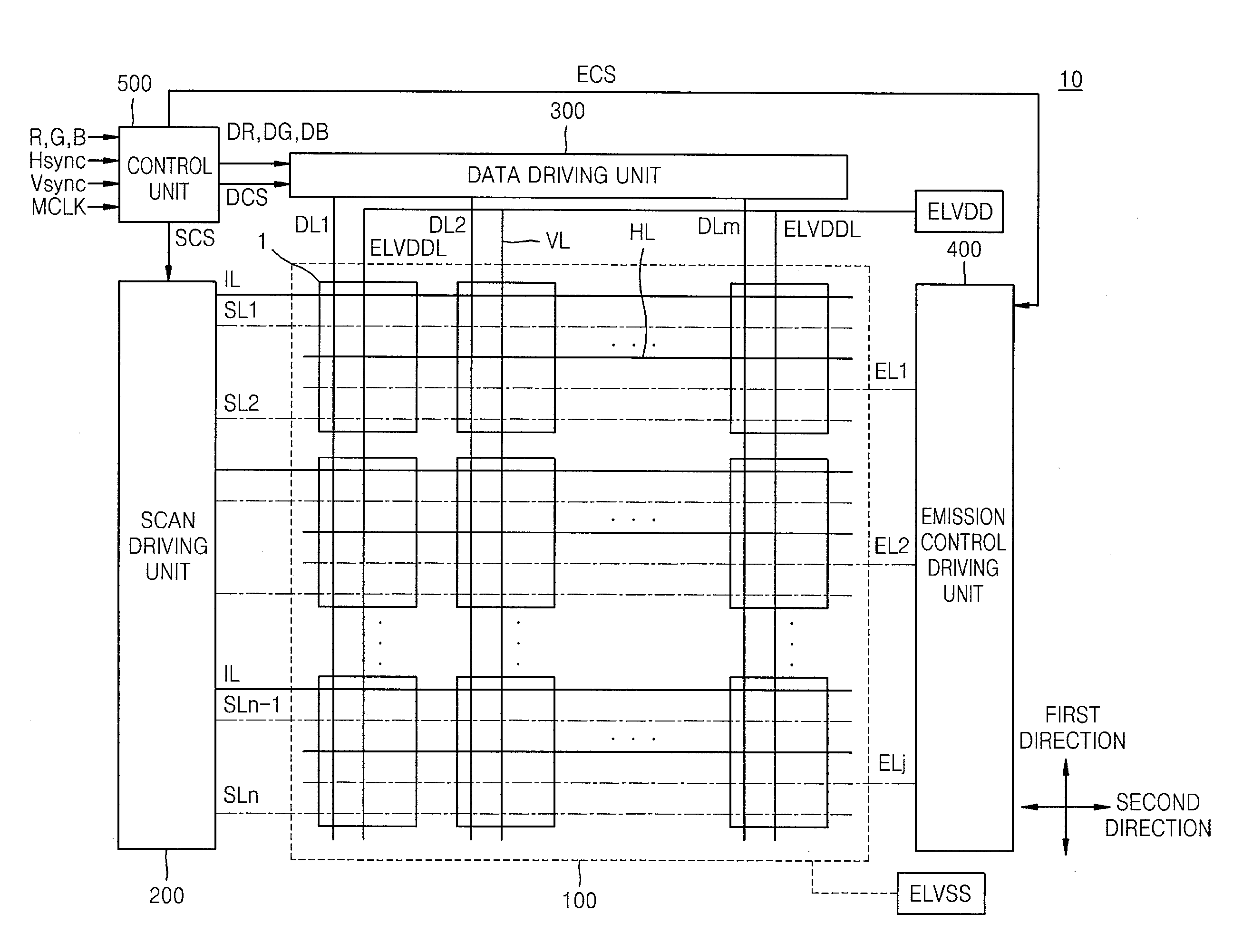
[0035]Hereinafter, embodiments of the present invention will be described in detail by explaining exemplary embodiments of the invention with reference to the attached drawings. The invention may, however, be embodied in many different forms, and should not be construed as being limited to the embodiments set forth herein; rather, these embodiments are provided so that this disclosure will be thorough and complete, and will fully convey the concept of the invention to those skilled in the art

[0036]In the following description, well-known functions or constructions are not described in detail to avoid obscuring the invention with unnecessary detail. Like reference numerals in the drawings denote like or similar elements throughout the specification.

[0037]Also, thicknesses and sizes of elements in the drawings may be arbitrarily shown for convenience of description, thus, the spirit and scope of the present invention are not necessarily defined by the drawings.

[0038]In the drawings, t...


PUM


Abstract

A thin film transistor array substrate includes a plurality of pixels, each of the pixels including a capacitor comprising a first electrode, and a second electrode located above the first electrode, a data line extending in a first direction, configured to provide a data signal, located above the capacitor, and overlapping a part of the capacitor, and a driving voltage line configured to supply a driving voltage, located between the capacitor and the data line, and comprising a first line extending in the first direction, and a second line extending in a second direction substantially perpendicular to the first direction.

Description

CROSS-REFERENCE TO RELATED APPLICATION[0001]This application claims priority to and the benefit of Korean Patent Application No. 10-2013-0022444, filed on Feb. 28, 2013, in the Korean Intellectual Property Office, the disclosure of which is incorporated herein in its entirety by reference.BACKGROUND[0002]1. Field[0003]Embodiments of the present invention relate to a thin film transistor array substrate and an organic light-emitting display apparatus including the same.[0004]2. Description of the Related Art[0005]An organic light-emitting display apparatus is self-emissive, and unlike a liquid crystal display apparatus, the organic light-emitting display apparatus does not require a separate light source, such as a backlight, thereby having comparatively reduced thickness and weight. Also, the organic light-emitting display apparatus has excellent characteristics including low power consumption, high brightness, a quick response time, or the like.[0006]The organic light-emitting disp...

Claims


Application Information

Patent Timeline
IPC IPC(8): H01L27/12H01L27/32
CPCH01L27/1255H01L27/3225H01L27/1237H10K59/1216H10K59/126H10K59/131H01L27/124
Inventor KO, MOON-SOONLEE, IL-JUNGIM, CHOONG-YOULKWON, DO-HYUNYOON, JU-WONWOO, MIN-WOO
Owner SAMSUNG DISPLAY CO LTD
Features
  • R&D
  • Intellectual Property
  • Life Sciences
  • Materials
  • Tech Scout
  • Unparalleled Data Quality
  • Higher Quality Content
  • 60% Fewer Hallucinations
Learn More