Semiconductor device and method of manufacturing the same

a technology of semiconductors and semiconductors, applied in the direction of semiconductor devices, basic electric elements, electrical equipment, etc., can solve the problem of electrical shorting of the underlying conductive film

Inactive Publication Date: 2015-07-30
KK TOSHIBA
View PDF4 Cites 24 Cited by
  • Summary
  • Abstract
  • Description
  • Claims
  • Application Information

AI Technical Summary

Problems solved by technology

Thus, the stopper film disposed below the bottom portion of a relatively shallow contact becomes excessively etched, so that the etching progresses through the stopper film and possibly electrically shorts the underlying conductive film.

Method used


Image

  • Semiconductor device and method of manufacturing the same
  • Semiconductor device and method of manufacturing the same
  • Semiconductor device and method of manufacturing the same

Examples


embodiments

[0030]Embodiments are described hereinafter with reference to the drawings. The drawings are schematic and thus, are not necessarily consistent with the actual correlation of thickness to planar dimensions and the actual thickness ratios between each of the layers. Thus, the same portion may be illustrated in different dimensions or ratios in different figures. Further, directional terms such as up, down, left, and right are used in a relative context with an assumption that the surface, on which circuitry is formed, of the later described semiconductor substrate faces up. Thus, the directional terms do not necessarily correspond to the directions based on gravitational acceleration. In the drawings referred to in the following description, elements that are identical or similar to those already illustrated or described are identified with identical or similar reference symbols and may not be re-described. Further, in the following description, XYZ orthogonal coordinate system is us...

first embodiment

[0031]A first embodiment will be described hereinafter with references to FIG. 1 to FIG. 9.

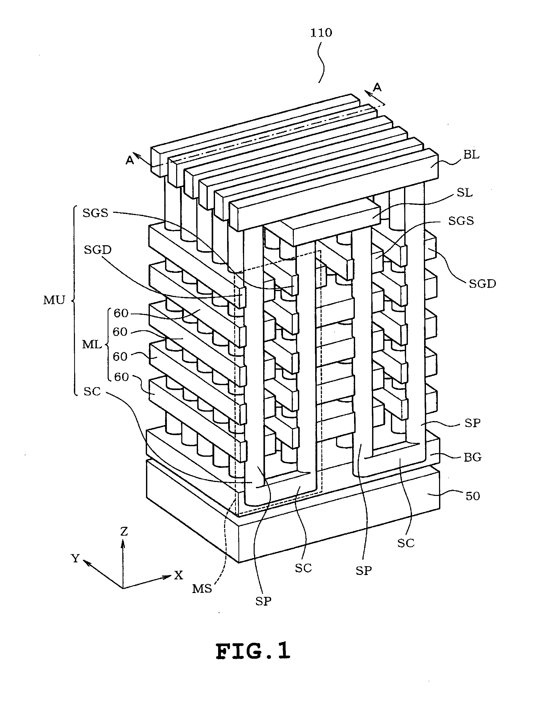
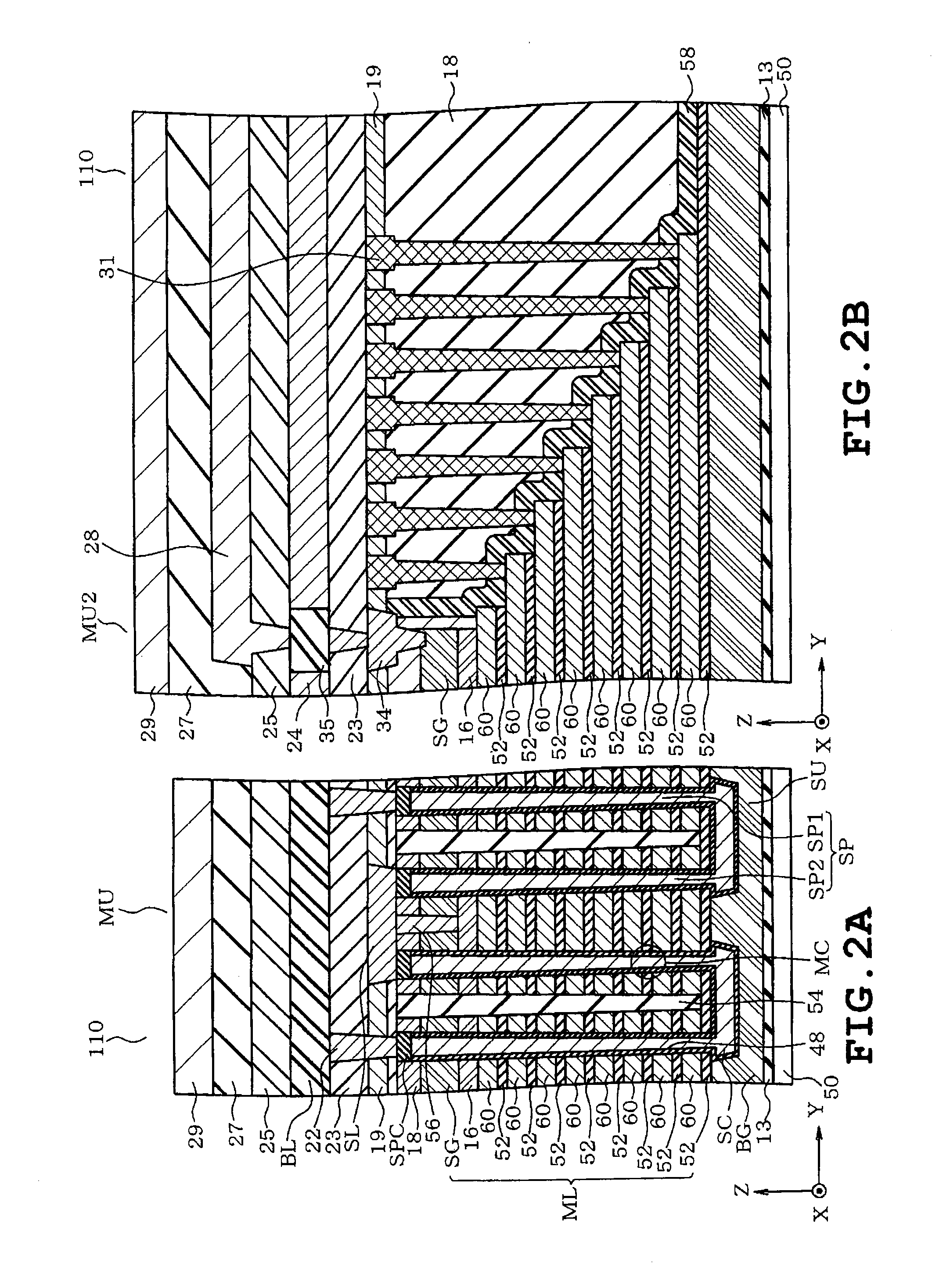
[0032]One example of a stacked-type nonvolatile semiconductor storage device is illustrated in FIG. 1, FIG. 2A, and FIG. 2B as one example of a semiconductor device. More specifically, the example of the stacked-type nonvolatile semiconductor storage device is configured as a NAND-type nonvolatile semiconductor storage device comprising a semiconductor substrate, conductive films, pillar electrodes, and electron trap films. The pillar electrodes are formed into pairs such that a couple of pillar electrodes are interconnected at their lower portions. Each pair of pillar electrodes is disposed orthogonal to the semiconductor substrate so as to extend through a stack of conductive films. An electron trap film is disposed between the pillar electrode and the conductive film, thereby forming a storage element.

[0033]FIG. 1 is one example of a perspective view schematically illustrating the structure...

second embodiment

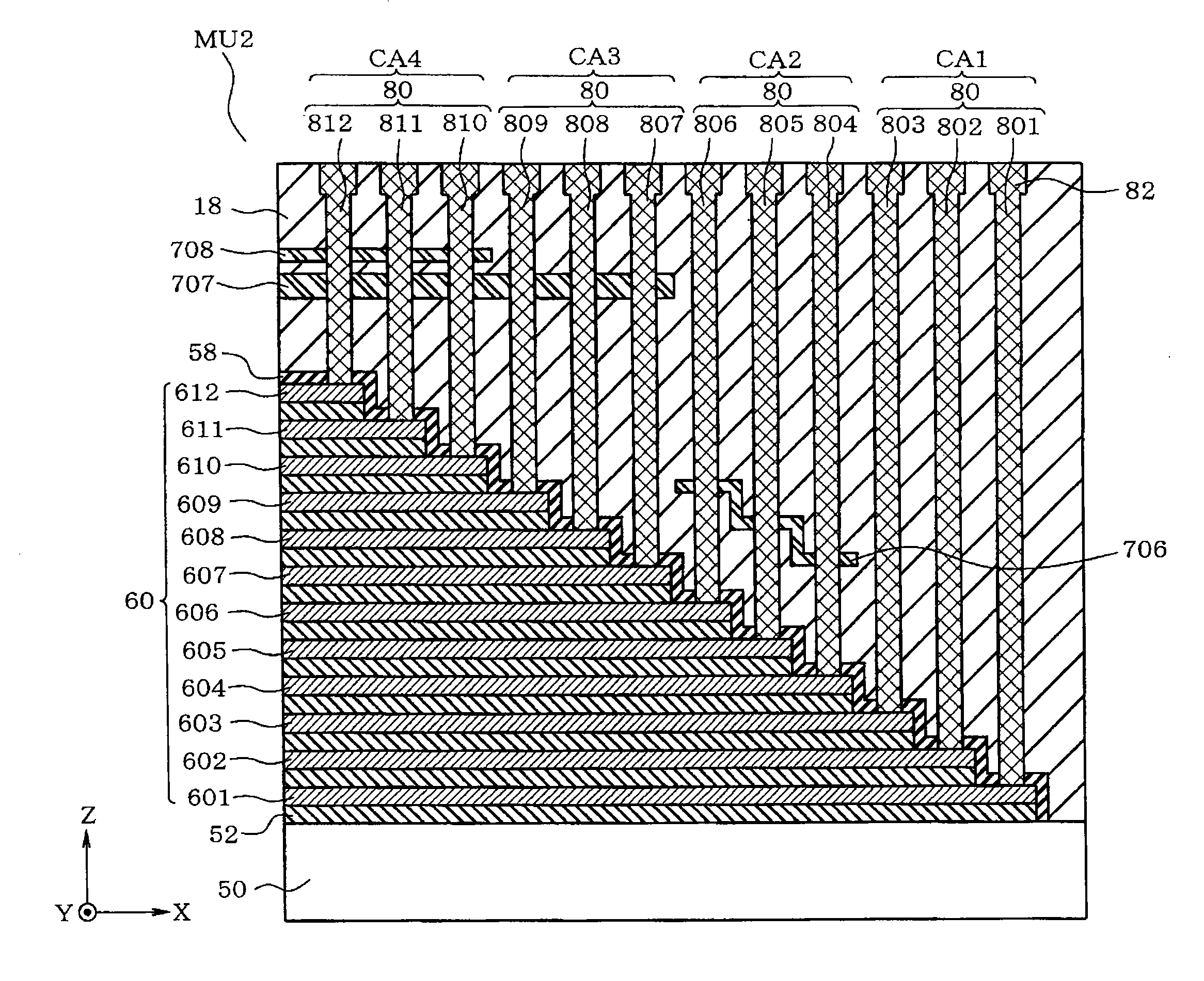
[0085]Next a description will be given on a second embodiment with reference to the drawings. FIG. 10 illustrates the second embodiment and is one example of a vertical cross-sectional view schematically illustrating the structure shaped like a stairway by conductive films 60 at wire connecting portion MU2 illustrated in FIG. 2B. FIG. 10 to FIG. 16 illustrate examples of 12 layers of conductive films 60 for convenience of explanation n; however, any number of conductive films 60 may be used.

[0086]In FIG. 10, twelve layers of conductive films 60 are provided as described above. Conductive film 60 in the lowermost layer is represented as conductive film 601, and subsequent layers are represented in sequence as conductive film 602, conductive film 603, and so forth, and conductive film 60 in the uppermost layer is represented as conductive film 612. Interelectrode insulating film 52 is provided between conductive films 60 for insulating conductive films 60. Conductive film 60 is formed...


PUM


Abstract

A semiconductor device includes a stack of conductive films, the stack of conductive films having a stairway portion located at an end portion thereof; an insulating layer disposed above the stack of conductive films; contact electrodes having different depths extending from an upper surface of the insulating layer to establish connection with upper surfaces of the conductive films in the stairway portion, the contact electrodes having different depths being arranged into at least a first contact group and a second contact group; an adjustment film disposed in the insulating layer; the contact electrodes in the second contact group extending through the adjustment film, a contact electrode having the smallest depth in the first contact group being deeper than a contact electrode having the greatest depth in the second contact group.

Description

CROSS-REFERENCE TO RELATED APPLICATION(S)[0001]This application is based upon and claims the benefit of priority from Japanese Patent Application No. 2014-011307, filed on, Jan. 24, 2014 the entire contents of which are incorporated herein by reference.FIELD[0002]Embodiments disclosed herein generally relate to a semiconductor device and a method of manufacturing the same.BACKGROUND[0003]When contacts, connecting to the upper surfaces of conductive films stacked in a stairway configuration, are formed simultaneously, the depths of the contact openings vary significantly between the lower layer films and the upper layer films of the stack. Thus, the stopper film disposed below the bottom portion of a relatively shallow contact becomes excessively etched, so that the etching progresses through the stopper film and possibly electrically shorts the underlying conductive film.BRIEF DESCRIPTION OF THE DRAWINGS[0004]FIG. 1 is one example of a perspective view schematically illustrating the...

Claims


Application Information

Patent Timeline
Patent Type & Authority Applications(United States)
IPC IPC(8): H01L21/768H01L27/115
CPCH01L27/115H01L21/76877H01L21/76816H01L21/76829H10B43/50H10B43/27
Inventor MATSUDA, YUYA
Owner KK TOSHIBA
Why Eureka
Try Eureka