

Thin film transistor substrate and display using the same
- Summary
- Abstract
- Description
- Claims
- Application Information
AI Technical Summary
Benefits of technology
Problems solved by technology
Method used
Image

Examples
first embodiment
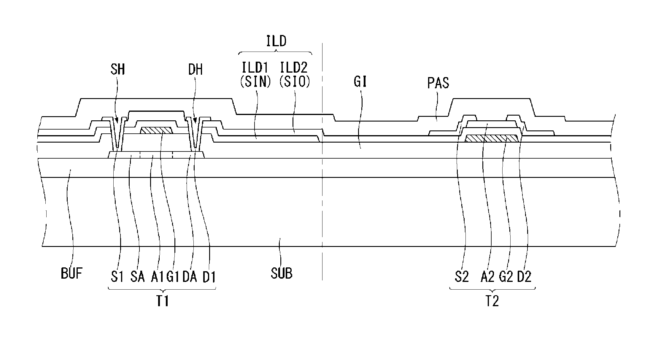
[0039]FIG. 1 is a cross sectional view illustrating a structure of a thin film transistor substrate for a flat panel display in which two different type thin film transistors are formed according to a first embodiment of the present disclosure. Here, the cross sectional views more clearly and conveniently show the main features of the present disclosure.
[0040]With reference to FIG. 1, the thin film transistor substrate for a flat panel display according to the first embodiment comprises a first thin film transistor T1 and a second thin film transistor T2 which are disposed on the same substrate SUB. The first and second thin film transistors T1 and T2 may be far apart from each other, or they may be disposed within a relatively close distance. Otherwise, these two thin film transistors are disposed as being overlapping each other.
[0041]On the whole surface of the substrate SUB, a buffer layer BUF is deposited. In some cases, the buffer layer BUF may not be included. Or, the buffer l...
second embodiment
[0073]FIG. 3 is a cross sectional view illustrating a structure of a thin film transistor substrate for a flat panel display in which two different types of thin film transistors are formed according to a second embodiment of the present disclosure.
[0074]The thin film transistor substrate according to the second embodiment is similar to that of the first embodiment. One difference is that, in the FIG. 3 example, the first intermediate layer ILD1 may include two layers. For example, the first intermediate layer ILD1 may include a lower oxide layer SIO2 stacked on a nitride layer SIN.
[0075]By the post-thermal process, the hydrogen particles in the nitride layer SIN may be diffused into the first semiconductor layer A1. Considering the hydrogenation efficiency, the nitride layer SIN may have a thickness of 1,000 Ř3,000 Å. As the oxide layer SIO2 of the first intermediate insulating layer ILD1 may compensate for a damaged surface condition of the gate insulating layer GI during the pat...
third embodiment
[0093]FIG. 5 is a cross sectional view illustrating a structure of a thin film transistor substrate for a flat panel display in which two different type thin film transistors are formed according to the third embodiment of the present disclosure.
[0094]The thin film transistor substrate according to the third embodiment is similar to that of the first and the second embodiments. One difference is that the first intermediate insulating layer ILD1 includes an oxide layer SIO, and the second intermediate insulating layer ILD2 includes a nitride layer SIN. For example, the second intermediate layer ILD2, including the nitride layer SIN, may not cover the second area where the second thin film transistor T2 is disposed, but may selectively cover the first area where the first thin film transistor T1 is disposed.
[0095]Located between the second gate electrode G2 and the second semiconductor layer A2, the first intermediate insulating layer ILD1 may act as a gate insulating layer for the se...
PUM
 Abstract
Description
Claims
Application Information