Organic light emitting display device

a light-emitting diode and display device technology, applied in the field of display devices, can solve the problems of image distortion between divided regions, analog driving techniques may not accurately implement the desired gray level, etc., and achieve the effect of reducing luminance changes and reducing image distortion

Active Publication Date: 2016-03-03
SAMSUNG DISPLAY CO LTD
View PDF2 Cites 25 Cited by
  • Summary
  • Abstract
  • Description
  • Claims
  • Application Information

AI Technical Summary

Benefits of technology

[0030]As described above, the OLED display device according to example embodiments of the present invention may reduce a luminance change caused by a frequency change of the clock signal for EMI minimization by inserting a vertical blank period into a frame period, thereby reducing image distortion. The OLED display device according to example embodiments of the present invention may calculate a luminance level of a next frame or may determine an image effect of the next frame in the vertical blank period.

Problems solved by technology

However, the analog driving technique may not accurately implement a desired gray level because the analog driving technique uses the voltage (i.e., an analog value) stored in the storage capacitor of each pixel.
However, image distortion may occur between divided regions.

Method used


Image

  • Organic light emitting display device
  • Organic light emitting display device
  • Organic light emitting display device

Examples


Embodiment Construction

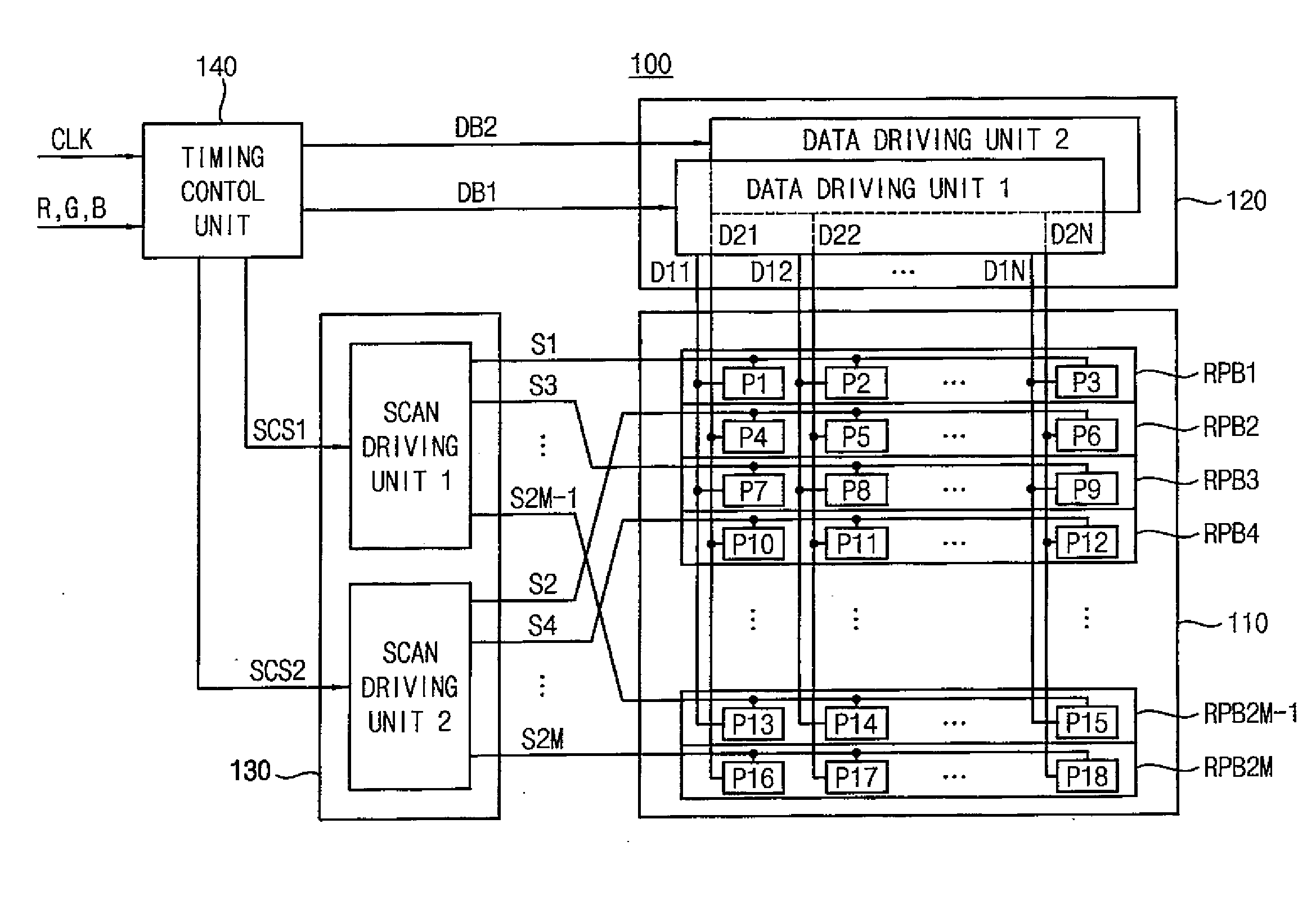
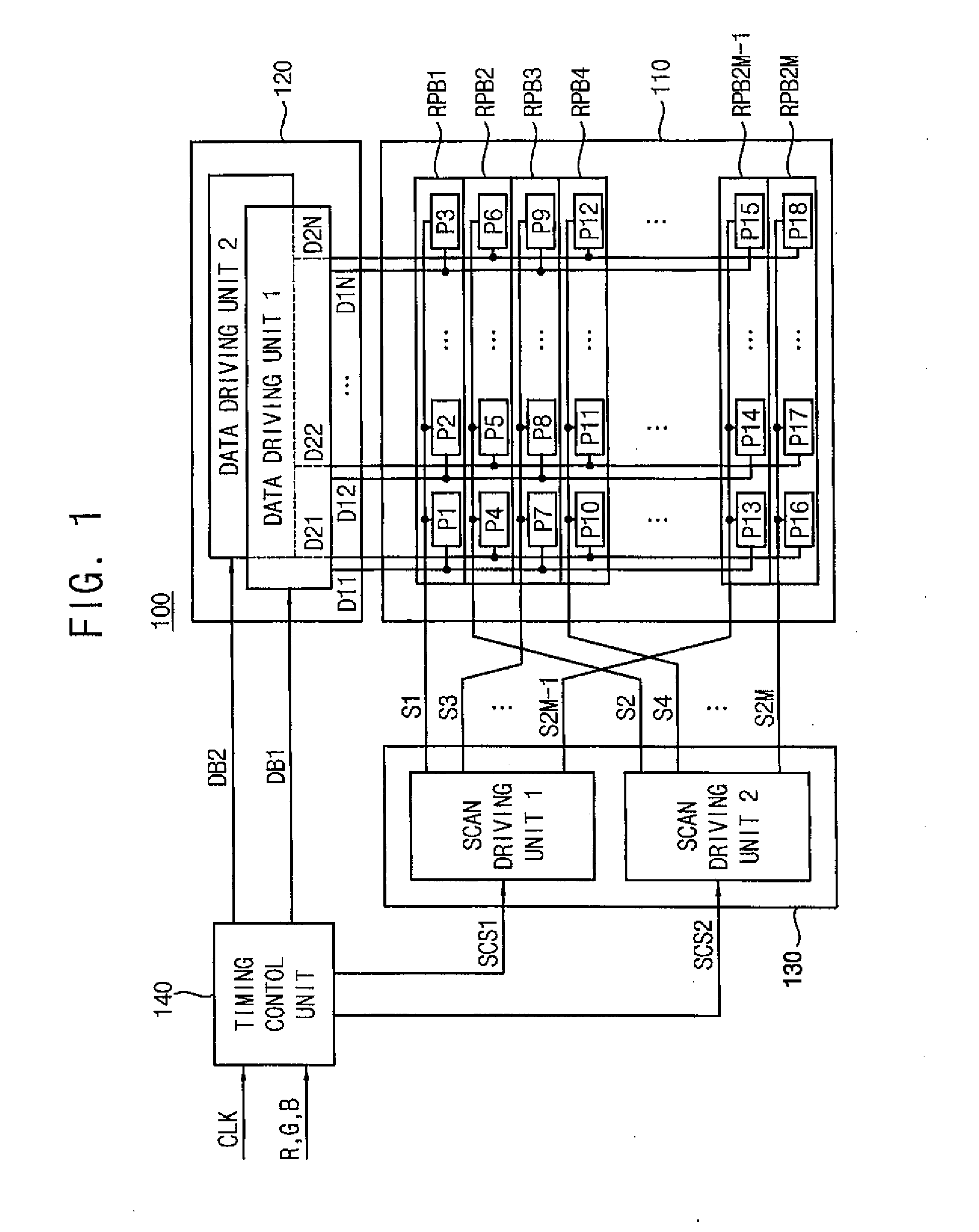
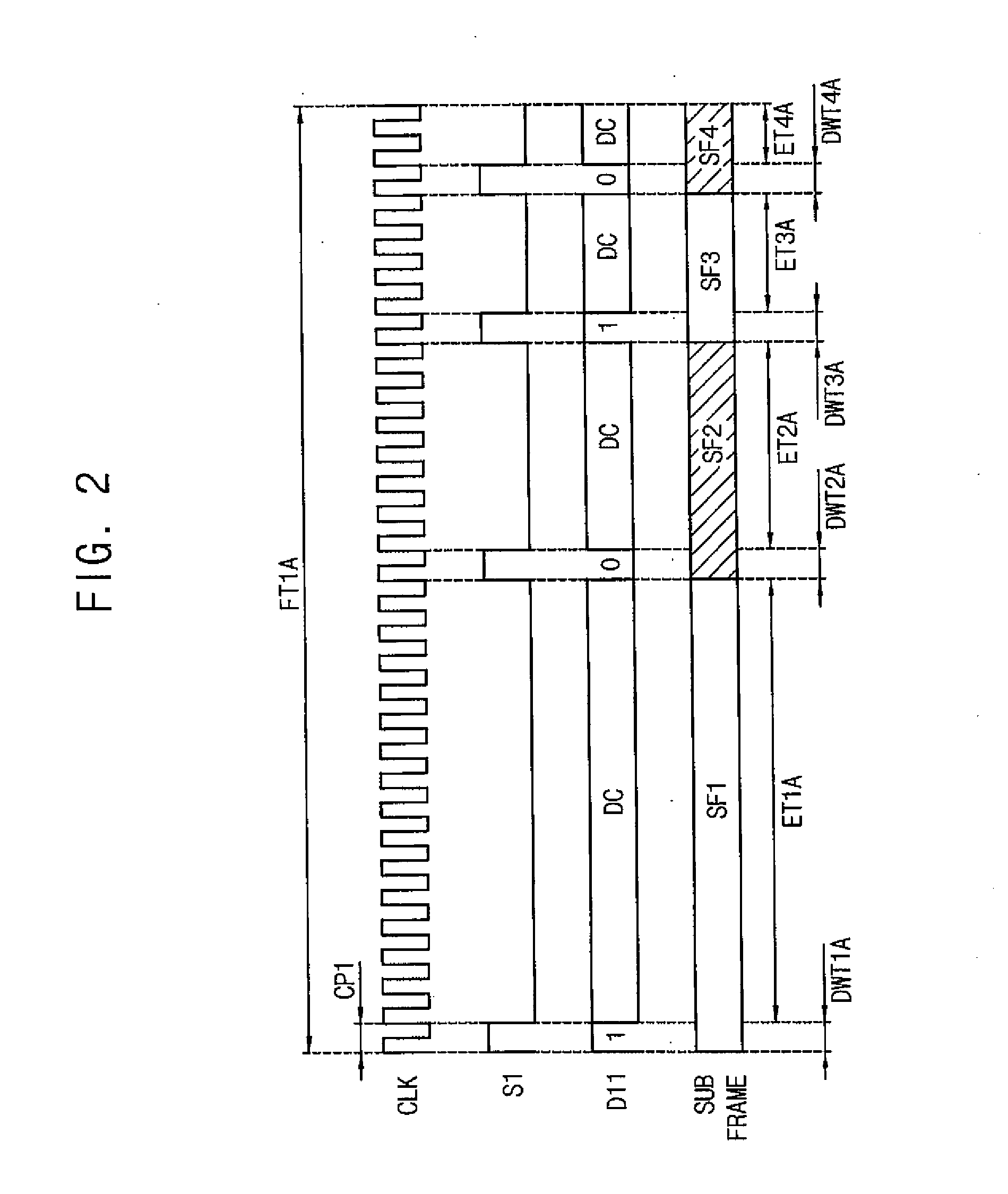
[0043]Various example embodiments of the present invention will be described more fully hereinafter with reference to the accompanying drawings, in which some example embodiments are shown. The present invention may, however, be embodied in many different forms and should not be construed as limited to the example embodiments set forth herein. Rather, these example embodiments are provided so that this disclosure will be thorough and complete, and will fully convey the scope of the present invention to those skilled in the art. In the drawings, the sizes and relative sizes of layers and regions may be exaggerated for clarity. Like numerals refer to like elements throughout.

[0044]It will be understood that, although the terms first, second, third, etc. may be used herein to describe various elements, these elements should not be limited by these terms. These terms are used to distinguish one element from another. Thus, a first element discussed below could be referred to instead as a...


PUM


Abstract

An organic light emitting diode (OLED) display device includes: a display panel including a first through (2M)-th row pixel blocks; a data driver including a first data driving unit to provide N odd row data signals to (2K−1)-th row pixel blocks and a second data driving unit to provide N even row data signals to (2K)-th row pixel blocks; a scan driver including a first scan driving unit configured to provide (2K−1)-th scan signals to (2K−1)-th row pixel blocks and a second scan driving unit configured to provide (2K)-th scan signals to (2K)-th row pixel blocks. The first frame period includes an activation period and a vertical blank period. The first scan driving unit is configured to activate the (2K−1)-th scan signals sequentially in pulse form in an activation period.

Description

CROSS-REFERENCE TO RELATED APPLICATION[0001]This application claims priority to and the benefit of Korean Patent Application No. 10-2014-0117289, filed on Sep. 3, 2014 in the Korean Intellectual Property Office (KIPO), the content of which is incorporated herein in its entirety by reference.BACKGROUND[0002]1. Field[0003]Example embodiments of the present invention relate generally to a display device. More particularly, embodiments of the present invention relate to an organic light emitting diode (OLED) display device with reduced image distortion.[0004]2. Description of the Related Art[0005]Organic light emitting diode (OLED) display devices have been widely used recently as flat display devices included in electronic devices, which are getting smaller and consuming less power. Generally, an OLED display device implements (i.e., displays) a specific gray level using a voltage stored in a storage capacitor of each pixel (i.e., an analog driving technique for an OLED display device)...

Claims


Application Information

Patent Timeline
Patent Type & Authority Applications(United States)
IPC IPC(8): G09G5/18G09G3/32
CPCG09G3/3266G09G5/18G09G3/2022G09G2310/0205G09G2310/0216
Inventor PYO, DONG-HAKLEE, JAE-HOON
Owner SAMSUNG DISPLAY CO LTD
Why Eureka
Try Eureka