Modulation device, light emitting device, and light emission system

a technology of light emitting devices and modules, applied in the direction of digital transmission, electromagnetic transceivers, instruments, etc., can solve the problems of lack of convenience, inability to use standalone devices, and the plurality of lighting devices

Active Publication Date: 2016-12-08
PANASONIC INTELLECTUAL PROPERTY MANAGEMENT CO LTD
View PDF2 Cites 3 Cited by
  • Summary
  • Abstract
  • Description
  • Claims
  • Application Information

AI Technical Summary

Benefits of technology

[0012]According to the present disclosure, a modulation device can be achieved that is suitable for a light emitting device convenient due to its capab...

Problems solved by technology

However, with the techniques disclosed in Japanese Unexamined Patent Application Publication No. 2013-110599, the plurality of lighting devices included in the light emission system require the visible light communication signal output device, and cannot transmit the ID themselves alone.
Stated differently, with the techniques disclosed ...

Method used


Image

  • Modulation device, light emitting device, and light emission system
  • Modulation device, light emitting device, and light emission system
  • Modulation device, light emitting device, and light emission system

Examples


embodiment 1

[0031]First, the light emitting device according to Embodiment 1 of the present disclosure will be described.

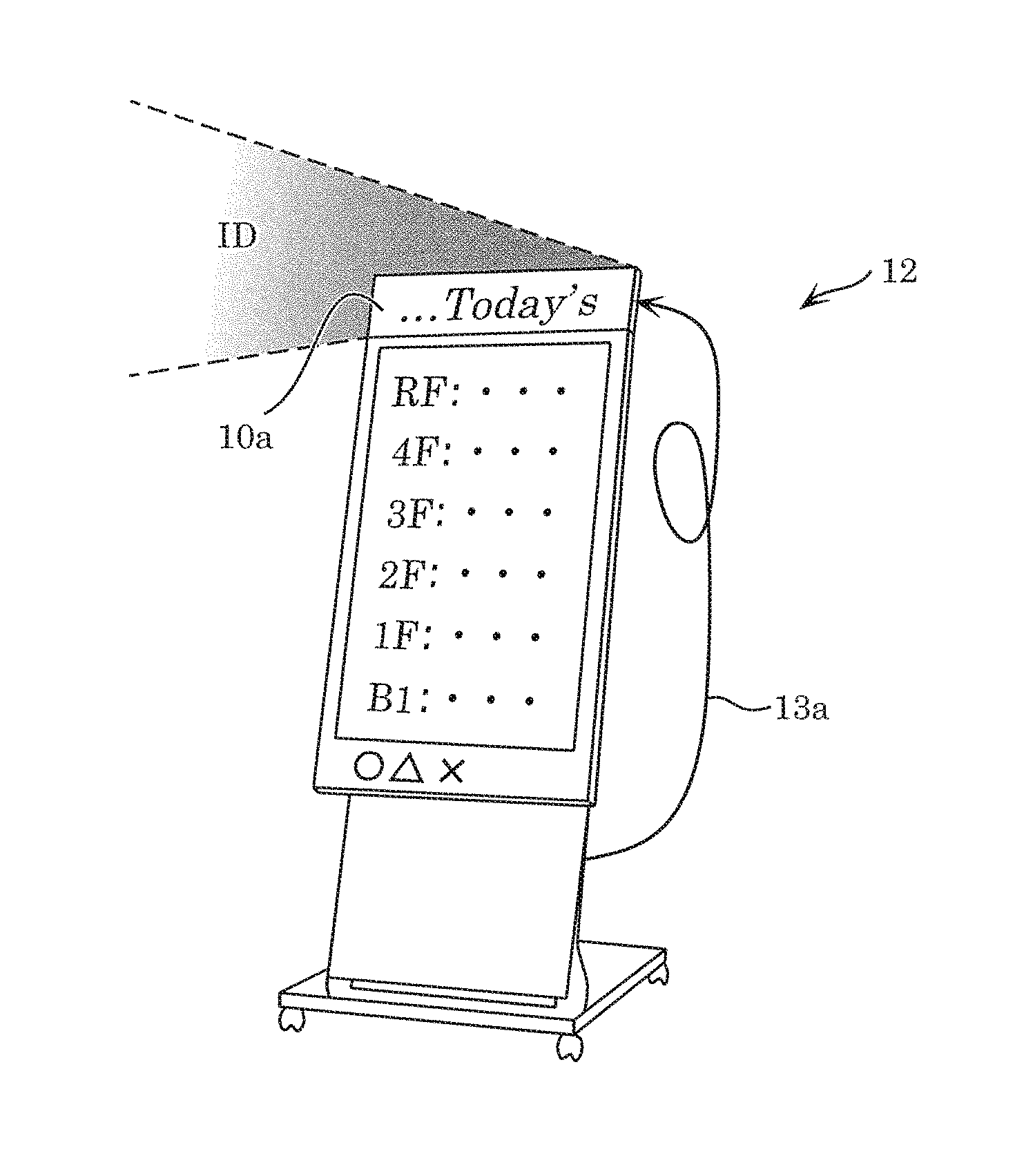
[0032]FIG. 1 illustrates a usage example of light emitting device 10a according to Embodiment 1. In the example illustrated, light emitting device 10a is provided at the top portion of electronic sign 12, and signal line 13a for inputting an ID from an external source (i.e., an external ID) into light emitting device 10a is connected to light emitting device 10a. Light emitting device 10a is, for example, a light emitting device capable of performing visible light communication, and is recognizable to a person as an electronic sign or lighting device.

[0033]As illustrated, when an external ID is input via the connected signal line 13a, light emitting device 10a transmits the input external ID via light communication. However, during a period in which the external ID is not received through signal line 13a or when signal line 13a is not connected to light emitting device 10a, l...

embodiment 2

[0057]Next, the light emitting device according to Embodiment 2 of the present disclosure will be described.

[0058]FIG. 4 illustrates a usage example of light emitting device 10b according to Embodiment 2. Here, light emission system 15 including light emitting device 10b configured of two lighting devices connected together by signal line 13a is illustrated. Signal line 13a is a cable for inputting the internal ID output from a first light emitting device 10b functioning as the master device, into a second light emitting device 10b functioning as a slave device, as an external ID. Stated differently, via signal line 13a, the internal ID stored in storage included in the first light emitting device 10b is input into the modulator circuit of the first light emitting device 10b, and that internal ID is input into the second light emitting device 10b as an external ID.

[0059]With light emission system 15 configured as described above, the same ID (“ID1” in FIG. 4) is transmitted in synch...

embodiment 3

[0084]Next, operations performed by the light emitting device according to Embodiment 3 of the present disclosure will be described.

[0085]FIG. 10A is a block diagram of light emitting device 10c according to Embodiment 3, and FIG. 10B is a block diagram of light emission system 15 according to Embodiment 3. More specifically, FIG. 10A is a block diagram of a single light emitting device 10c, and FIG. 10B is a block diagram of light emission system 15 including a plurality of light emitting devices 10c illustrated in FIG. 10A and connected together via signal line 13a.

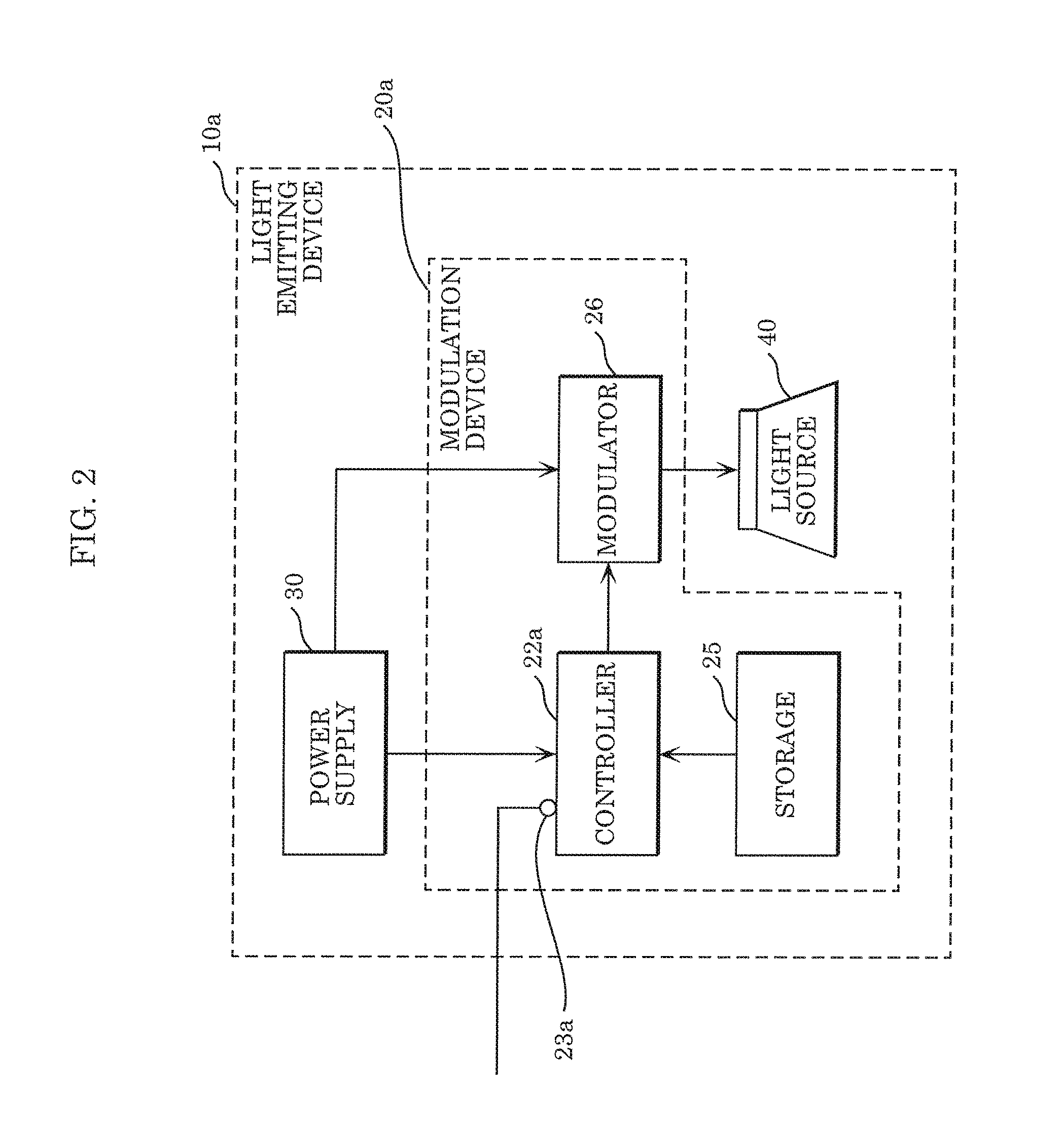
[0086]As illustrated in FIG. 10A, light emitting device 10c according to Embodiment 3 includes power supply 30, light source 40, and modulation device 20c. Modulation device 20c includes control circuit 22c, storage 25, modulator circuit 26, and transceiver 29. Light emitting device 10c and modulation device 20c according to Embodiment 3 have similar configurations as Embodiment 1. However, in Embodiment 3, modulation ...


PUM


Abstract

A modulation device includes a modulator circuit that causes a light source to perform light communication, storage storing an internal ID, and a control circuit that determines whether an external ID is input into the modulation device. When the control circuit determines that the external ID is input into the modulation device, the control circuit causes the input external ID to be input, as a modulation signal, into the modulator circuit. When the control circuit determines that the external ID is not input into the modulation device, the control circuit causes the internal ID stored in the storage to be input, as a modulation signal, into the modulator circuit.

Description

CROSS REFERENCE TO RELATED APPLICATION[0001]This application claims the benefit of priority of Japanese Patent Application Number 2015-112640 filed on Jun. 2, 2015 the entire content of which is hereby incorporated by reference.BACKGROUND[0002]1. Technical Field[0003]The present disclosure relates to a modulation device, light emitting device, and light emission system, and in particular to a modulation device used for light communication such as visible light communication.[0004]2. Description of the Related Art[0005]In light emission systems such as an electronic sign including a plurality of light emitting devices capable of light communication such as visible light communication, the plurality of light emitting devices are required to transmit the same identification information (ID) in synchronization. This is because even a light communication reception device located in a region in which light from the plurality of light emitting devices overlaps needs to be able to receive a...

Claims


Application Information

Patent Timeline
IPC IPC(8): H04B10/116H04B10/516H04L7/00H05B37/02H04B10/40
CPCH04B10/116H05B37/0209H04B10/516H04L7/0075H04B10/40G08C17/02H05B47/10H04B10/50H05B47/165
Inventor MATSUKAWA, YOSHIHIKOKIDO, SHOJIROU
Owner PANASONIC INTELLECTUAL PROPERTY MANAGEMENT CO LTD
Why Eureka
Try Eureka