Semiconductor package structure and method for forming the same

a semiconductor and package technology, applied in the direction of semiconductor/solid-state device details, semiconductor devices, electrical devices, etc., can solve the problems of warpage, high fabrication cost, and too large package siz

Active Publication Date: 2017-03-23
MEDIATEK INC
View PDF10 Cites 58 Cited by
  • Summary
  • Abstract
  • Description
  • Claims
  • Application Information

AI Technical Summary

Problems solved by technology

Accordingly, the size of the package is too big and warpage is an issue of concern.
Accordingly, the fabrication cost is high

Method used


Image

  • Semiconductor package structure and method for forming the same
  • Semiconductor package structure and method for forming the same
  • Semiconductor package structure and method for forming the same

Examples


Embodiment Construction

[0019]The following description is of the best-contemplated mode of carrying out the invention. This description is made for the purpose of illustrating the general principles of the invention and should not be taken in a limiting sense. The scope of the invention is determined by reference to the appended claims.

[0020]The present invention will be described with respect to particular embodiments and with reference to certain drawings, but the invention is not limited thereto and is only limited by the claims. The drawings described are only schematic and are non-limiting. In the drawings, the size of some of the elements may be exaggerated for illustrative purposes and not drawn to scale. The dimensions and the relative dimensions may or may not correspond to actual dimensions in the practice of the invention.

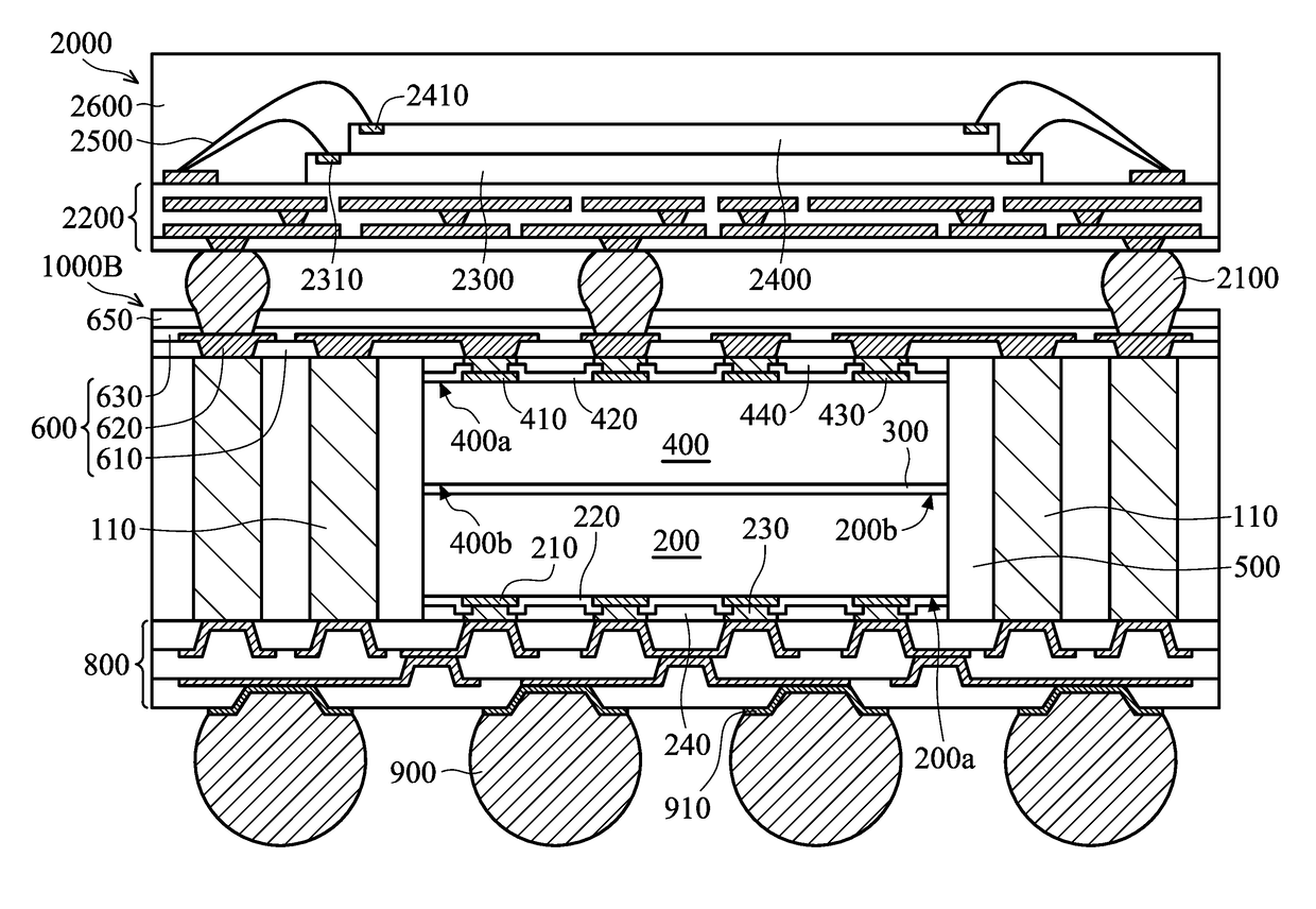
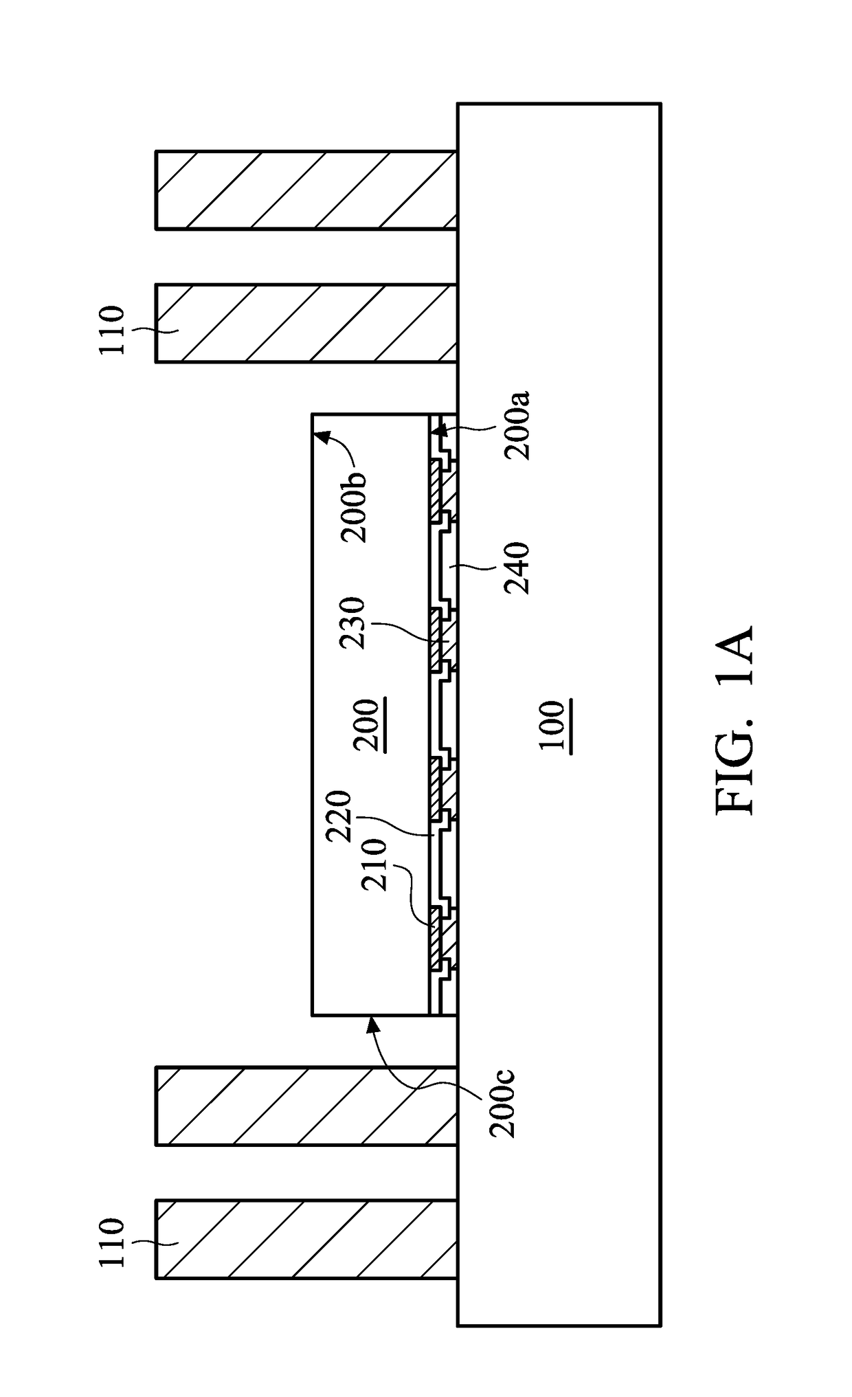
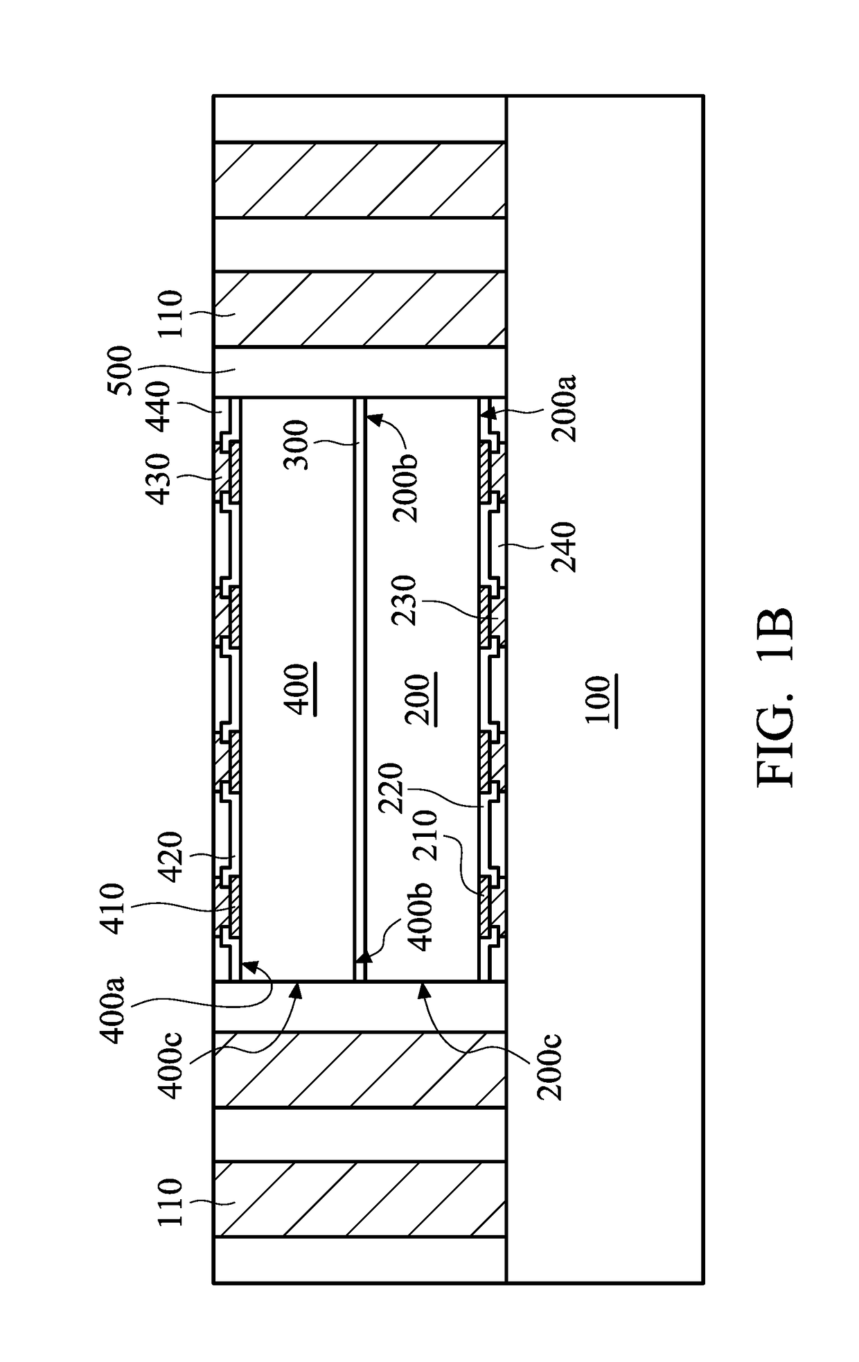
[0021]FIGS. 1A-1E are cross-sectional views of various stages of a method for forming a semiconductor package structure, in accordance with some embodiments of the disclosure....


PUM


Abstract

A semiconductor package structure is provided. The semiconductor package structure includes a first semiconductor die including a first active surface and a first non-active surface. The semiconductor package structure also includes a second semiconductor die including a second active surface and a second non-active surface. The second semiconductor die is stacked on the first semiconductor die. The first non-active surface faces the second non-active surface. The semiconductor package structure further includes a first redistribution layer (RDL) structure. The first active surface faces the first RDL structure. In addition, the semiconductor package structure includes a second RDL structure. The second active surface faces the second RDL structure.

Description

CROSS REFERENCE TO RELATED APPLICATIONS[0001]This Application claims the benefit of U.S. Provisional Application No. 62 / 222,439 filed on Sep. 23, 2015, the entirety of which is incorporated by reference herein.BACKGROUND OF THE INVENTION[0002]Field of the Invention[0003]The present invention relates to a semiconductor package structure, and in particular to a multi-die semiconductor package structure and methods for forming the same.[0004]Description of the Related Art[0005]With the continued development of electronics industries, such as those related to the 3Cs (Computer, Communications and Consumer electronics), there has been rapidly increasing consumer demand for devices that are multi-functional, more convenient, and smaller. This demand has driven the need for increased integrated circuit (IC) density. Increased input-output (I / O) pin count and increased demands for IC density have led to the development of multi-die packages. With demands for high performance and high integr...

Claims


Application Information

Patent Timeline
IPC IPC(8): H01L25/10H01L23/31H01L21/683H01L25/00H01L21/56H01L23/538H01L23/00
CPCH01L25/105H01L2224/02373H01L23/3128H01L24/32H01L24/09H01L25/50H01L21/565H01L21/6835H01L24/83H01L2225/1035H01L2225/1041H01L2225/06548H01L2224/48091H01L2225/0652H01L2225/06568H01L2224/08111H01L2224/0401H01L23/5389H01L21/50H01L23/488H01L25/04H01L2225/04H01L21/568H01L24/19H01L24/20H01L25/0657H01L2224/04042H01L2224/04105H01L2224/12105H01L2224/32145H01L2224/32225H01L2224/48227H01L2224/73265H01L2224/73267H01L2224/92244H01L2225/0651H01L2225/1058H01L2924/14H01L2924/1421H01L2924/1431H01L2924/1432H01L2924/14335H01L2924/1434H01L2924/1436H01L2924/15311H01L2924/3511H01L23/49816H01L23/5383H01L23/5384H01L2221/68345H01L2221/68359H01L2221/68372H01L2224/19H01L2924/00012H01L2924/00014H01L2924/00H01L2224/83005
Inventor KUO, CHE-HUNGCHOU, CHE-YA
Owner MEDIATEK INC
Why Eureka
Try Eureka