Fan out wafer level package using silicon bridge

a silicon bridge and wafer technology, applied in the direction of semiconductor devices, semiconductor/solid-state device details, electrical equipment, etc., can solve the problems of high interconnect density requirements, wire bonding interconnection, substrate interconnection, etc., and achieve the effect of reducing the number of rdls

Inactive Publication Date: 2015-12-17
APPLE INC
View PDF6 Cites 64 Cited by
  • Summary
  • Abstract
  • Description
  • Claims
  • Application Information

AI Technical Summary

Problems solved by technology

The increasing demand of memory bandwidth presents selected challenges to the signal integrity of memory channels within semiconductor packages.
In such configurations, certain semiconductor device packages have thin profile and high interconnect density requirements that do not allow the use of traditional interconnection approaches between the die.
For example, wire bonding interconnection, substrate interconnection, or post fabrication redistribution layer (RDL) interconnection may not be suitable for providing a high interconnect density while maintaining a desired thin profile in the semiconductor device package.

Method used


Image

  • Fan out wafer level package using silicon bridge
  • Fan out wafer level package using silicon bridge
  • Fan out wafer level package using silicon bridge

Examples


Embodiment Construction

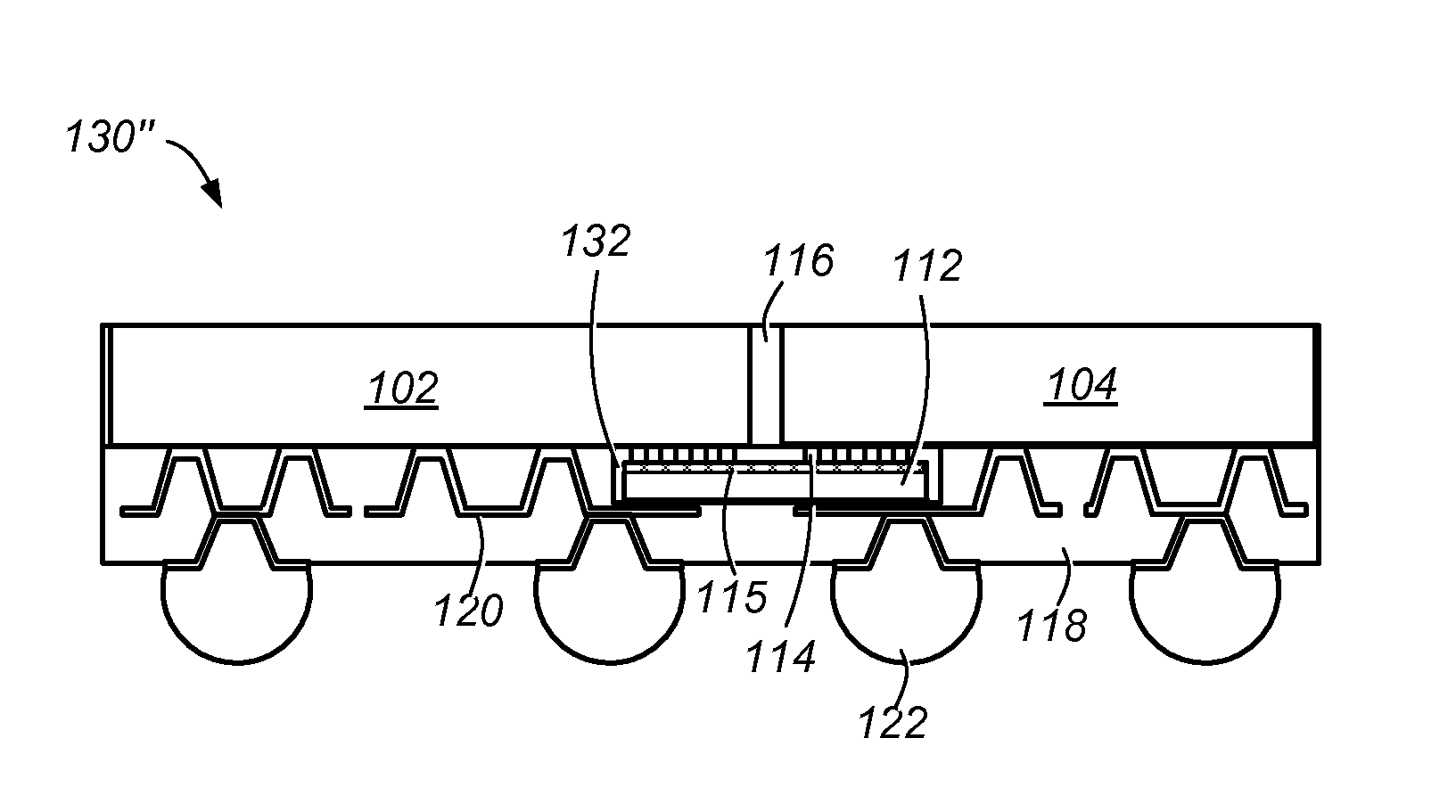
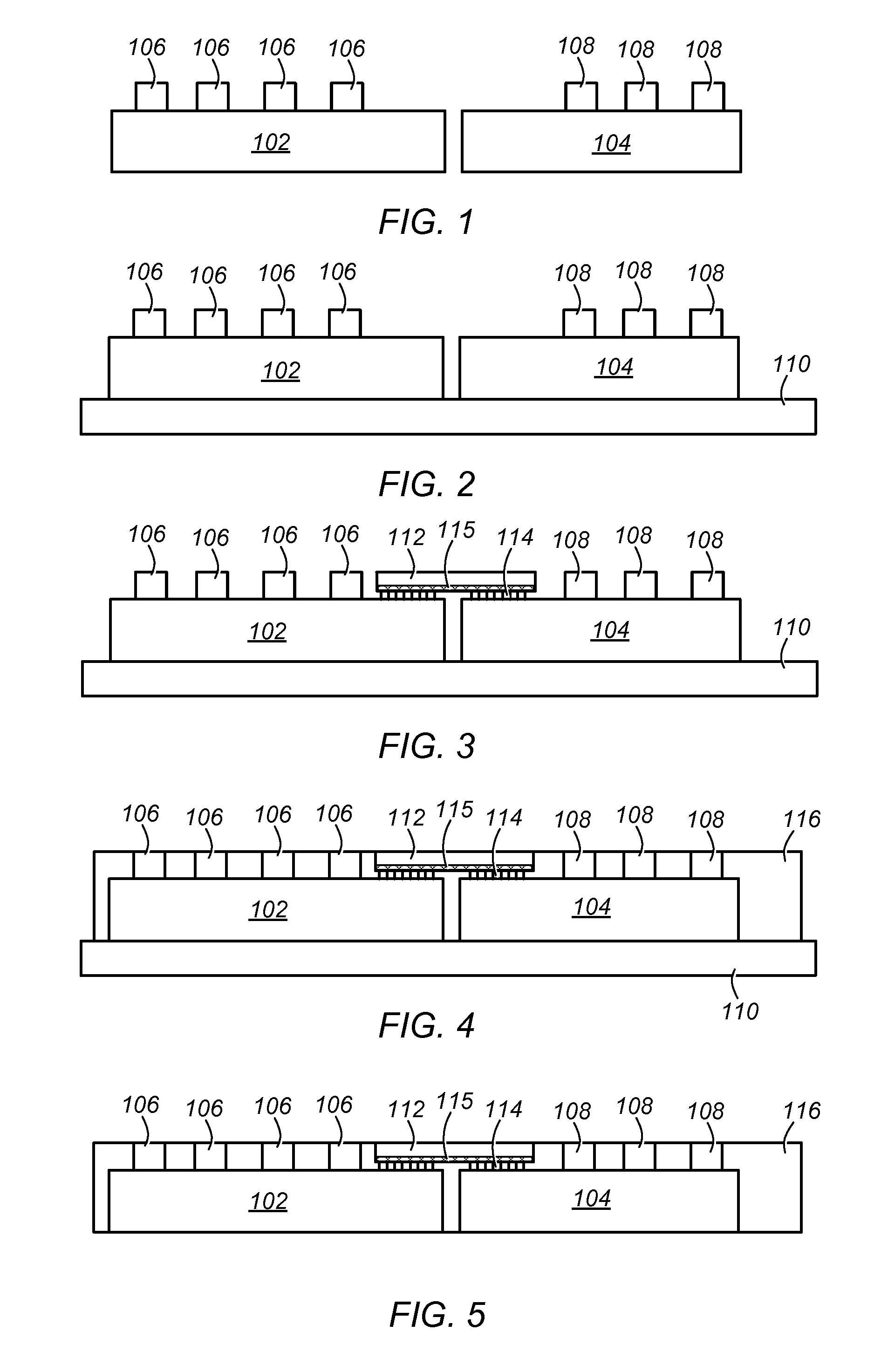
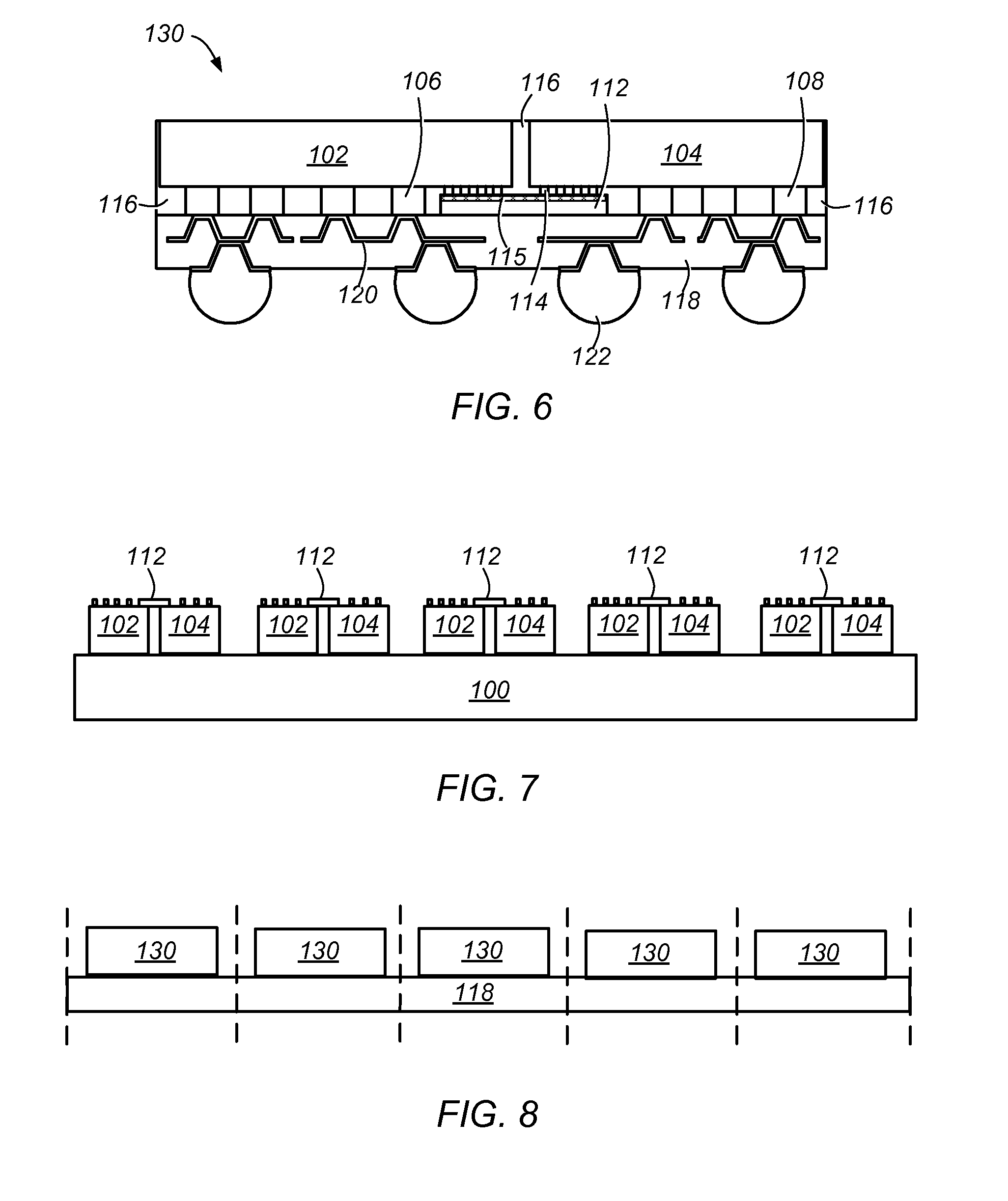
[0024]FIGS. 1-6 depict cross-sectional representations of an embodiment of a simplified process flow for forming a semiconductor device package. FIG. 1 depicts a cross-sectional representation of logic die 102 and memory die 104. Logic die 102 may be, for example, a system on a chip (“SoC”). In some embodiments, logic die 102 is a flip chip logic die. In certain embodiments, memory die 104 is a DDR (double data rate) die (e.g., an 8 GB DDR die). In some embodiments, memory die 104 is a flip chip memory die. In some embodiments, memory die 104 is a discrete memory die. In some embodiments, memory die 104 includes two or more memory die (e.g., vertically stacked memory die).

[0025]In certain embodiments, terminals 106 are formed on logic die 102 and terminals 108 are formed on memory die 104. Terminals 106 and 108 may be formed on active sides of logic die 102 and memory die 104, respectively. Terminals 106 and terminals 108 may be formed on their respective die while the die are on th...


PUM


Abstract

A semiconductor device package includes a logic die coupled to a memory die in a side-by-side configuration on a redistribution layer (e.g., the logic die and the memory die are substantially adjacent). A silicon bridge may be used to interconnect the logic die and the memory die. The silicon bridge may be positioned between the die and the redistribution layer. The silicon bridge and the redistribution layer may be coupled to the lower (active) surfaces of the logic die and the memory die. The package may be formed using a wafer level process that forms a plurality of packages simultaneously.

Description

PRIORITY CLAIM[0001]This patent claims priority to U.S. Provisional Patent Application No. 62 / 011,840 to Zhai et al., entitled “FAN OUT WAFER LEVEL PACKAGE USING SILICON BRIDGE”, filed Jun. 13, 2014, which is incorporated by reference in its entirety.BACKGROUND[0002]1. Technical Field[0003]Embodiments described herein relate to semiconductor packaging and methods for packaging semiconductor devices. More particularly, the embodiments described herein relate to a package with a logic die and to a memory die interconnected inside a semiconductor device package.[0004]2. Description of Related Art[0005]The semiconductor industry continues to develop semiconductor packages to have lower cost, higher performance, increased integrated circuit density, and increased package density. Logic die (e.g., system on a chip (“SoC”)) and / or memory die continue to become more highly integrated, which requires increased interconnection density. Thus, interconnect pitch is being reduced further and fur...

Claims


Application Information

Patent Timeline
Patent Type & Authority Applications(United States)
IPC IPC(8): H01L23/538H01L23/31H01L21/56H01L25/00H01L21/768H01L23/00H01L25/18
CPCH01L23/5381H01L2924/1434H01L23/3178H01L24/08H01L25/18H01L25/50H01L21/768H01L21/563H01L21/568H01L23/5386H01L24/03H01L2924/381H01L2224/02331H01L2224/0239H01L2924/1431H01L24/81H01L23/3128H01L2224/92124H01L23/5389H01L24/19H01L2224/12105H01L2224/16227H01L2224/73209H01L2224/81005H01L2225/1035H01L2924/18161H01L2924/18162H01L23/49816H01L23/5385H01L24/16H01L24/24H01L24/73H01L2224/131H01L2224/13124H01L2224/13144H01L2224/13147H01L2224/1357H01L2224/136H01L2224/13611H01L2924/00014H01L2924/014
Inventor ZHAI, JUNHU, KUNZHONG
Owner APPLE INC
Why Eureka
Try Eureka