

Microwave antenna apparatus, packing and manufacturing method
a microwave antenna and microwave antenna technology, applied in the direction of antennas, waveguides, semiconductor devices, etc., can solve the problems of narrow bandwidth (1-5%), distorted radiation patterns, and high amount of parasitic radiation to all directions, so as to reduce the amount of parasitic radiation, improve radiation patterns, and increase the bandwidth
- Summary
- Abstract
- Description
- Claims
- Application Information
AI Technical Summary
Benefits of technology
Problems solved by technology
Method used
Image

Examples
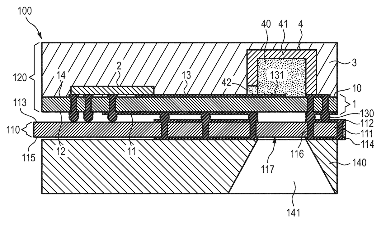
embodiment 1
2. Microwave antenna apparatus as defined in embodiment 1,
wherein the filling material is a foam-like filling material having a permittivity below 1.5.
3. Microwave antenna apparatus as defined in any preceding embodiment,
wherein the filling material comprises one or more of PCB material, mold material of the mold layer, material of the carrier, PTFE, PEN, PET, acryl.
4. Microwave antenna apparatus as defined in any preceding embodiment,
wherein the waveguide is open or closed on a side opposite to the side on which it is arranged on the first surface of the carrier layer.
5. Microwave antenna apparatus as defined in any preceding embodiment,
wherein the microstrip line is arranged on the first surface of the carrier layer and the ground plane is arranged on the second surface of the carrier layer and wherein the wave-guide comprises an opening on a side adjacent the first surface of the carrier layer, through which the microstrip line leads into the waveguide.
6. Microwave antenna appara...
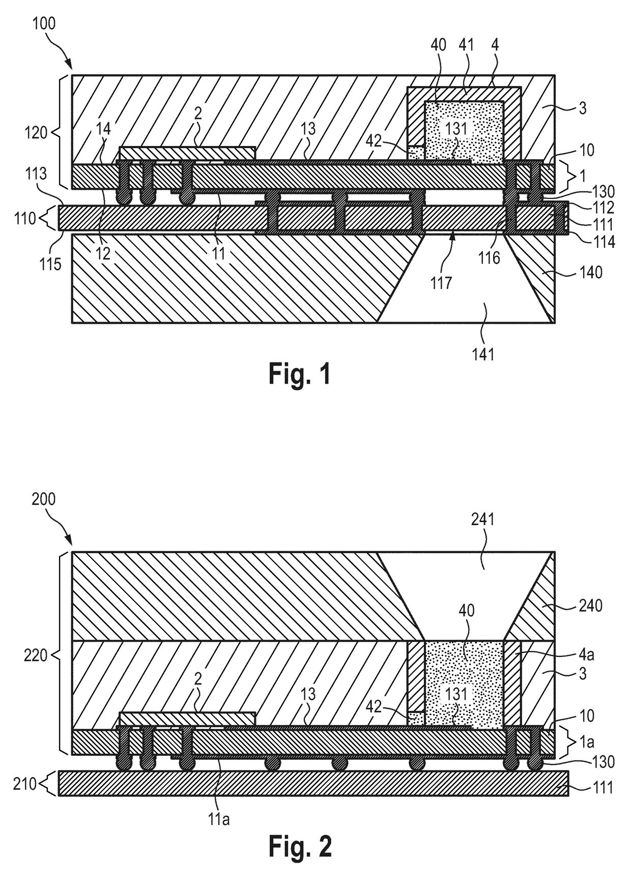
embodiment 13
14. Microwave antenna package as defined in embodiment 13,
wherein the microwave antenna apparatus is configured as defined in embodiment 1,
wherein the waveguide is closed on a side opposite to the side on which it is arranged on the first surface of the carrier layer and
wherein the PCB layer carries at least one contact layer on one surface, the contact layer being coupled to the semiconductor element via the coupling between the PCB arrangement and the microwave antenna apparatus, wherein a transmission area of the PCB layer facing the waveguide is free from the contact layer.
15. Microwave antenna package comprising
a PCB arrangement comprising a PCB layer carrying a first contact layer on a first surface and a second contact layer on a second surface opposite the first surface, wherein said contact layers are coupled by coupling elements arranged within the PCB layer, wherein a transmission area of the PCB layer is arranged between coupling elements and is free from the contact lay...
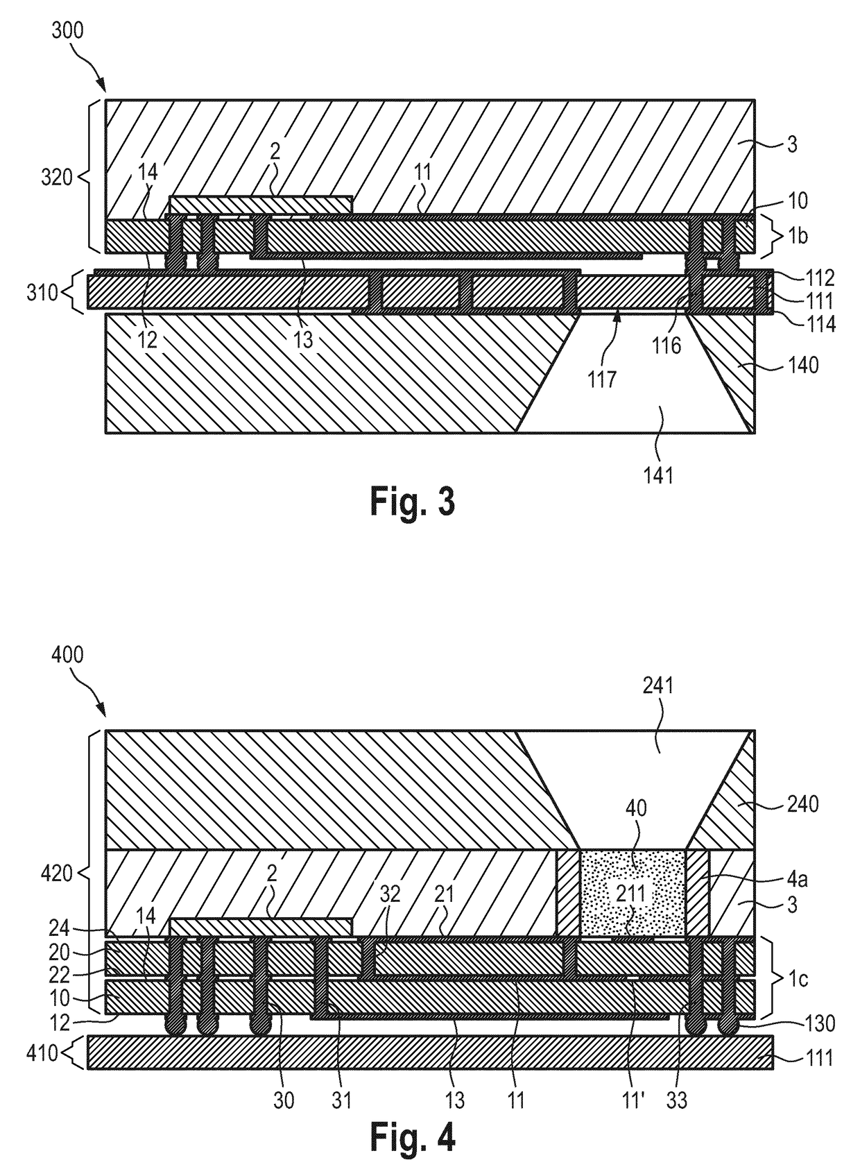
embodiment 15
16. Microwave antenna package as defined in embodiment 15,
wherein the redistribution layer comprises two or more carrier layers and one or more metal layers, wherein the ground plane is arranged between adjacent carrier layers, the microstrip line is arranged on a second outer surface of the redistribution layer opposite the first outer surface facing the PCB arrangement and a metal layer is arranged on the first outer surface of the redistribution layer, wherein the ground plane, the microstrip line and the one or more metal layers are configured to form an aperture coupled patch feed adjacent to the transmission area.
17. Microwave antenna package as defined in embodiment 15 or 16,
wherein the redistribution layer comprises two microstrip lines forming a differential line and a dipole antenna arranged at the end of the differential line adjacent the transmission area.
18. Microwave antenna package as defined in any one of embodiments 14 to 17,
further comprising a cover layer arranged...
PUM
 Abstract
Description
Claims
Application Information