Under bump metallurgy structure of a package and method of making same

a technology of bump metallurgy and semiconductor packaging, which is applied in the direction of semiconductor devices, semiconductor/solid-state device details, electrical apparatus, etc., can solve the problems of copper metal becoming brittle and more rigid, and the conventional technology of fine-pitch wire bonding structures cannot keep pace with demand,

Inactive Publication Date: 2008-07-17
ADVANCED CHIP ENG TECH +1
View PDF6 Cites 74 Cited by
  • Summary
  • Abstract
  • Description
  • Claims
  • Application Information

AI Technical Summary

Benefits of technology

[0008]A metallization structure for a semiconductor integrated circuit package has a semiconductor integrated circuit die, with a bonding pad formed thereon. A first dielectric layer having a first opening is formed over the die. A first metal layer is formed within the first opening and over the bonding pad, and extends over the first dielectric layer. A redistributed metal layer is formed within

Problems solved by technology

As integrated circuits (IC) advance toward higher speeds and larger pin counts, conventional technologies for achieving fine-pitch wire bonding structures cannot keep pace with the demand resulting from increased IC chip processing speeds and higher IC chip pin counts due to traditional wire bonding technologies that have approached or even reached their limits.
However, existing UBM schemes have been designed to optimize metallurgical or processing parameters rather than to improve th

Method used


Image

  • Under bump metallurgy structure of a package and method of making same
  • Under bump metallurgy structure of a package and method of making same
  • Under bump metallurgy structure of a package and method of making same

Examples


Embodiment Construction

[0015]The present invention discloses an under bump metallurgy structure for semiconductor package of a die and method of the same. It can also be applied to a wafer level package. Some sample embodiments of the invention will now be described in greater detail. Nevertheless, it should be recognized that the present invention can be practiced in a wide range of other embodiments besides those explicitly described, and the scope of the present invention is expressly not limited expect as specified in the accompanying claims.

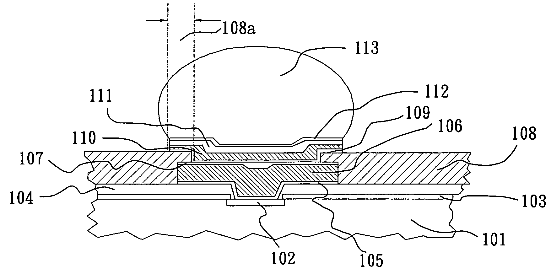
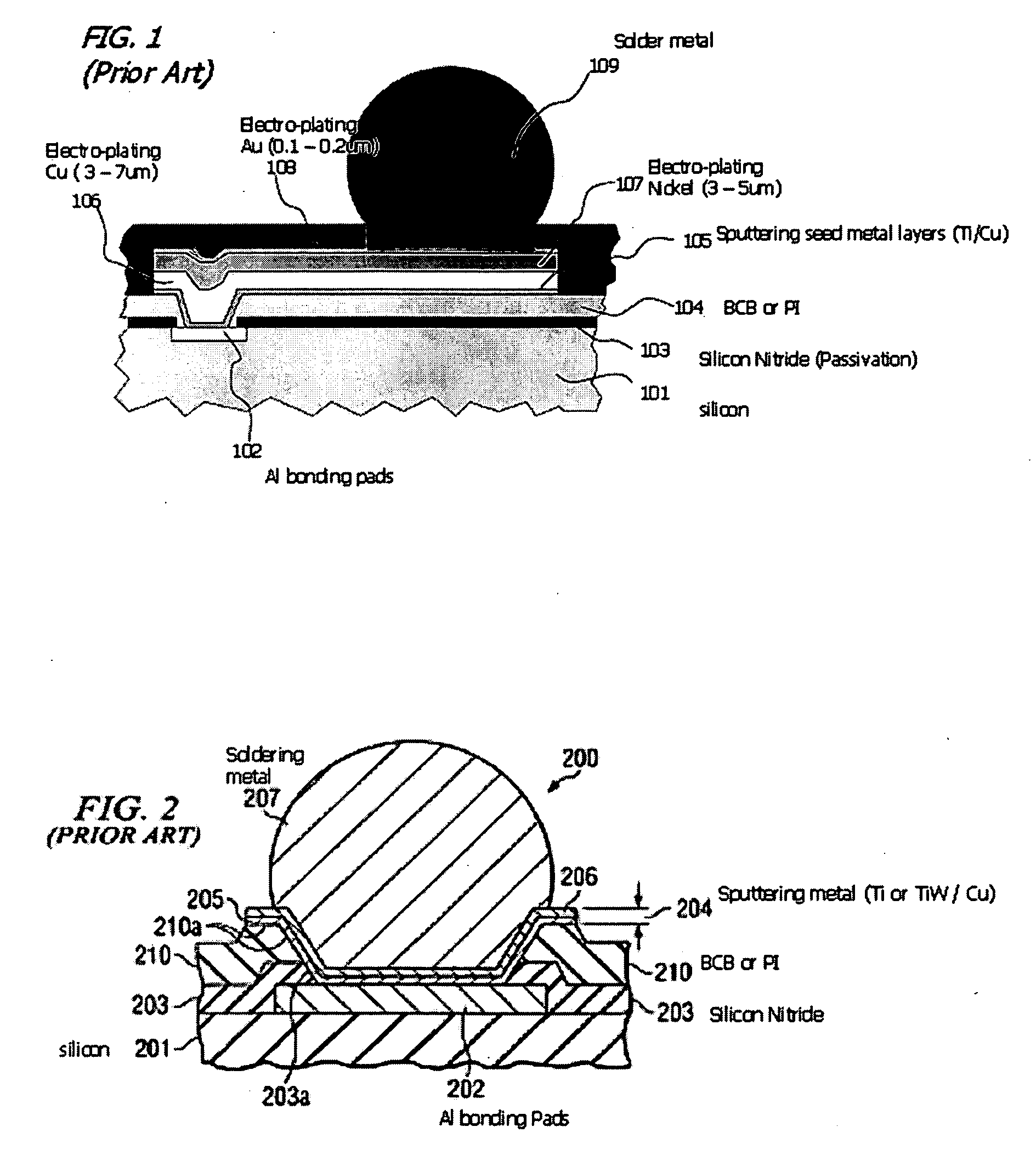
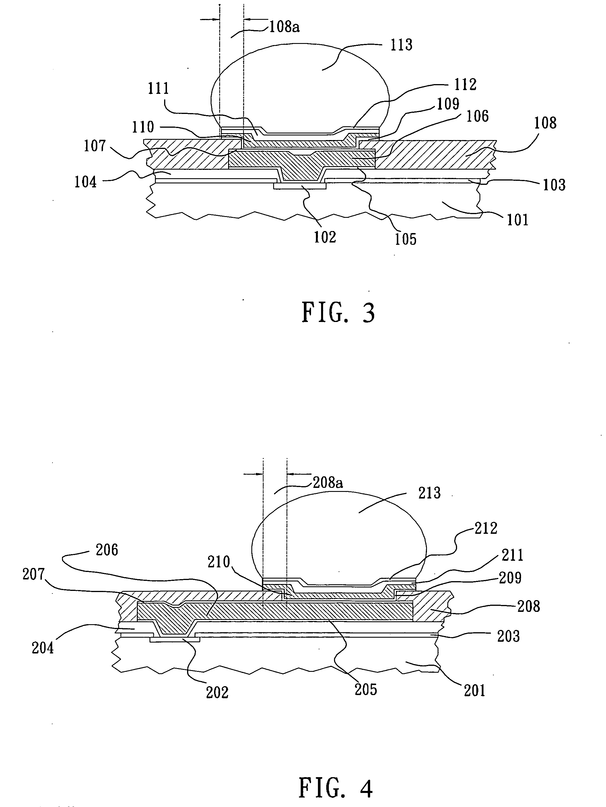
[0016]A new Under Bump Metallurgy (UBM) layer is disclosed herein which is especially suitable for use with a Wafer Level Chip Scale Package (WLCSP). The UBM dramatically improves package lifetime, and also avoids tin infiltration issue. The mechanical properties of the solder joint is further improved by providing a larger area of contact between the material of the UBM and the solder material, thereby improving the integrity of the solder-UBM interface. In the c...


PUM


Abstract

A package for a semiconductor integrated circuit die comprises a redistributed layer formed over a first barrier layer electrically connected to a bonding pad of a die. A second barrier layer is formed over the redistributed layer. A multi-metal layer is formed over the second barrier layer for coupling to a solder ball, wherein the multi-metal layer has an extending part that extends outside a second opening over the upper of the second dielectric layer to prevent tin infiltration from the solder ball to the redistribution layer.

Description

TECHNICAL FIELD[0001]The present invention relates to an under bump metallurgy (UBM) structure in a semiconductor package, and more particularly, to a UBM scheme to prevent tin infiltration.BACKGROUND OF THE INVENTION[0002]As integrated circuits (IC) advance toward higher speeds and larger pin counts, conventional technologies for achieving fine-pitch wire bonding structures cannot keep pace with the demand resulting from increased IC chip processing speeds and higher IC chip pin counts due to traditional wire bonding technologies that have approached or even reached their limits. As such, the current trend is to replace wire bonding structures with other package structures and assembly, such as a flip chip packages and a wafer level packages (WLP).[0003]Some chip bonding technologies utilize a copper bump attached to a contact pad on the chip to make an electrical connection for signal input and output. For instance, new packaging methods include BGA (Ball Grid Array) and CSP (Chip...

Claims


Application Information

Patent Timeline
IPC IPC(8): H01L23/495H01L21/00
CPCH01L24/03H01L2924/0002H01L2224/0401H01L2224/05083H01L2224/05624H01L2924/01004H01L2924/01013H01L2924/01014H01L2924/01015H01L2924/01022H01L2924/01028H01L2924/01029H01L2924/01033H01L2924/01047H01L2924/0105H01L2924/01051H01L2924/01073H01L2924/01074H01L2924/01075H01L2924/01078H01L2924/01079H01L2924/01082H01L2924/01322H01L2924/01327H01L2924/014H01L2924/05042H01L2924/14H01L2924/3025H01L24/05H01L2224/05584H01L2224/05027H01L2224/03828H01L24/13H01L2224/02331H01L2224/03462H01L2224/0347H01L2224/05008H01L2224/05022H01L2224/0508H01L2224/05111H01L2224/05139H01L2224/05147H01L2224/05155H01L2224/05171H01L2224/05644H01L2224/1132H01L2224/11334H01L2224/1147H01L2224/11849H01L2224/13111H01L2924/00013H01L2924/01006H01L2924/01024H01L2224/05572H01L2924/00014H01L2224/13099H01L2224/05099H01L2224/13599H01L2224/05599H01L2224/29099H01L2224/29599H01L2224/05552
Inventor FANG, SYCHYIYANG, WEN KUNTSAI, CHEN LUNG
Owner ADVANCED CHIP ENG TECH
Why Eureka
Try Eureka