Semiconductor devices and fabrication methods thereof

a technology of semiconductor devices and fabrication methods, applied in the direction of semiconductor devices, semiconductor/solid-state device details, electrical apparatus, etc., can solve the problems of increasing electrical resistance, increasing power consumption, and reducing the processing speed of semiconductor dies

Active Publication Date: 2010-11-30
AMKOR TECH SINGAPORE HLDG PTE LTD
View PDF22 Cites 77 Cited by
  • Summary
  • Abstract
  • Description
  • Claims
  • Application Information

AI Technical Summary

Problems solved by technology

Further, the use of the conductive wires for the connection of the semiconductor dies and the substrate or the connection of the respective semiconductor dies via conductive patterns increases the overall length of interconnection lines, inevitably leading to an increase in electrical resistance.
Moreover, since the conductive wires are employed as the interconnection lines, the processing speed of the semiconductor dies is reduced, resulting in an increase in power consumption.

Method used


Image

  • Semiconductor devices and fabrication methods thereof
  • Semiconductor devices and fabrication methods thereof
  • Semiconductor devices and fabrication methods thereof

Examples


Embodiment Construction

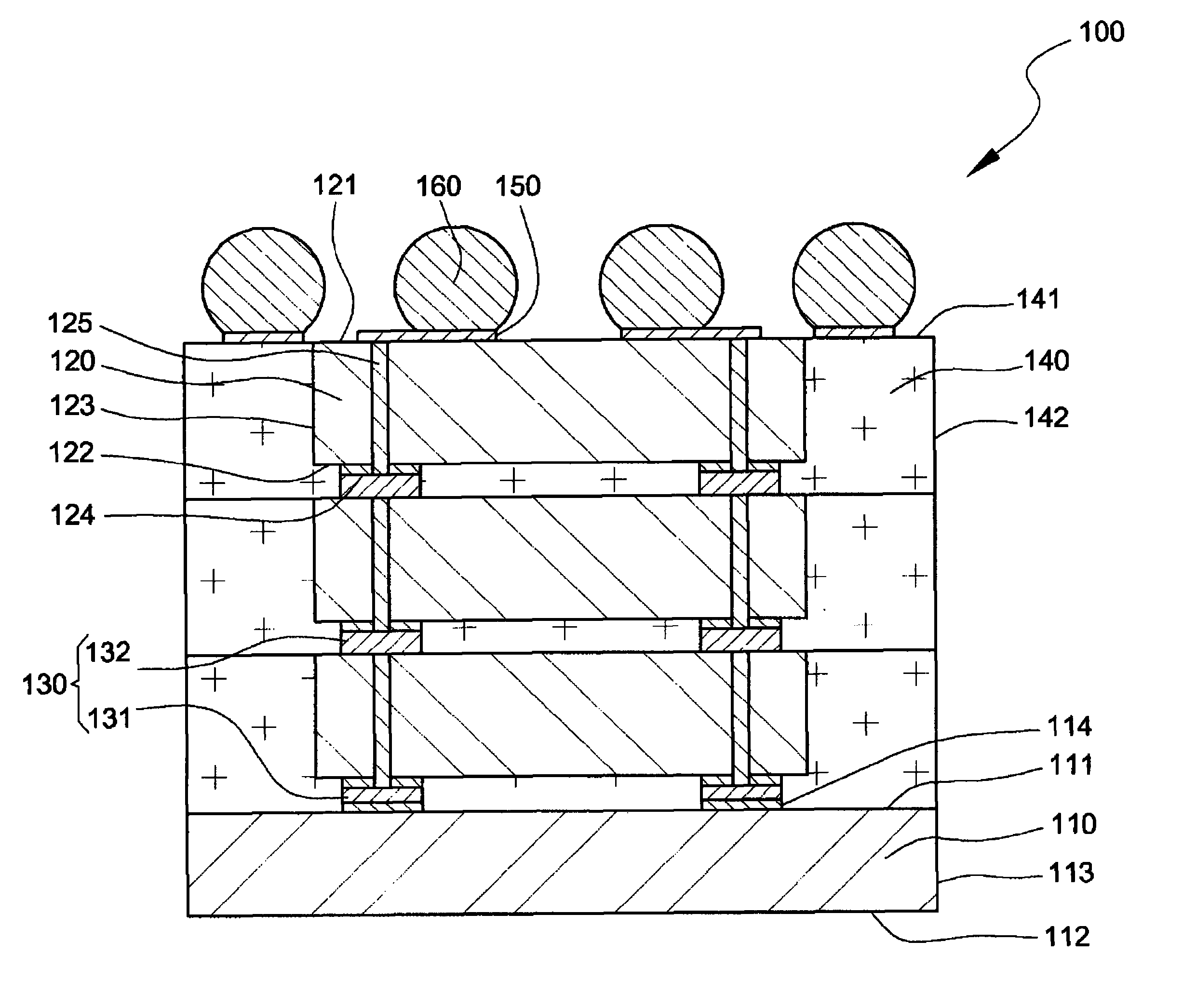
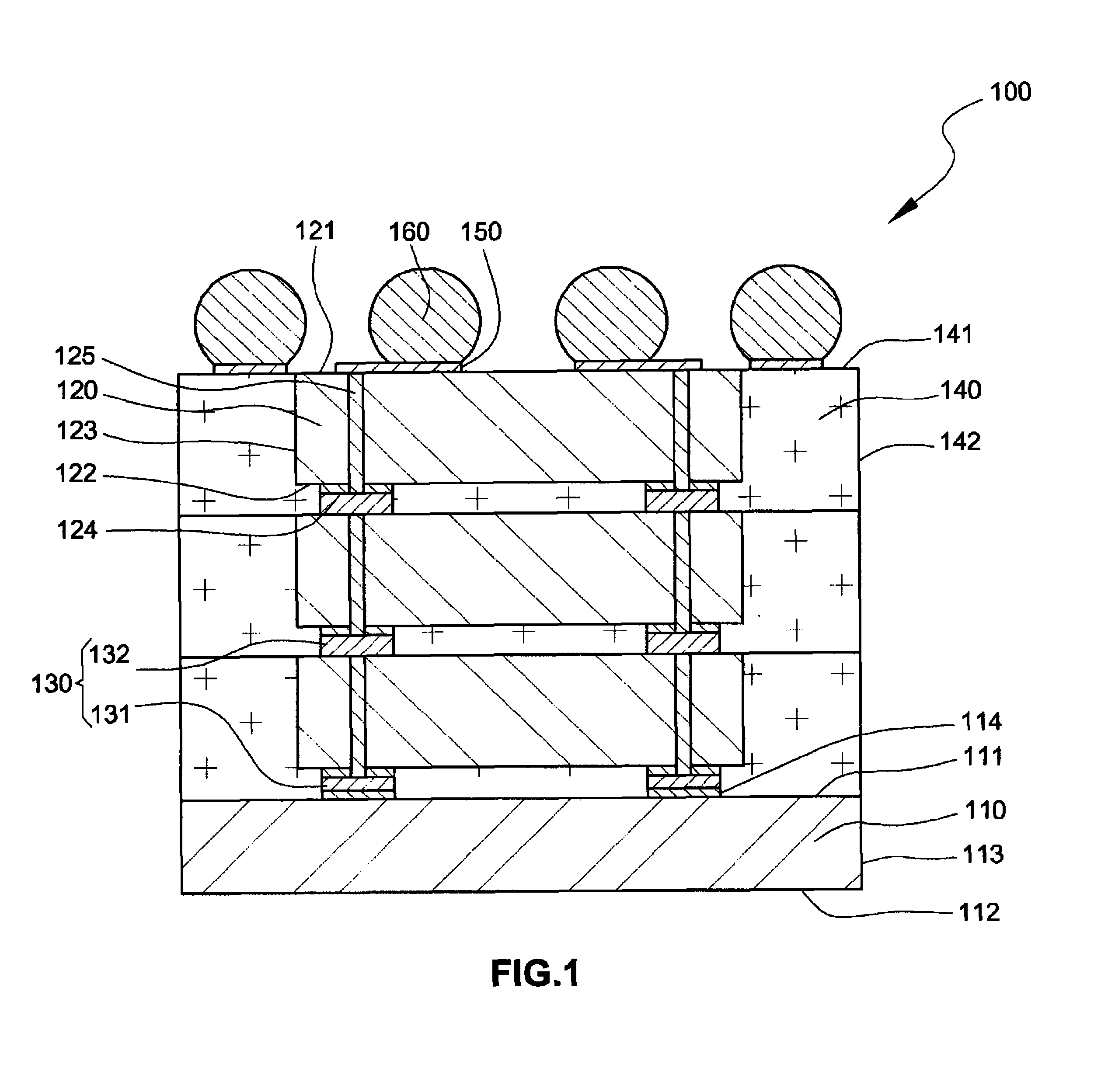
[0016]Referring to FIG. 1, there is illustrated a cross-sectional view of a semiconductor device 100 according to an embodiment of the present invention.

[0017]As illustrated in FIG. 1, the semiconductor device 100 comprises a first semiconductor die 110, a plurality of second semiconductor dies 120 stacked on the first semiconductor die 110, a plurality of conductive connection members 130, an encapsulant 140, a plurality of redistribution layers 150 and a plurality of solder balls 160.

[0018]The first semiconductor die 110 has an approximately planar first surface 111, an approximately planar second surface 112 opposed to the first surface 111, and approximately planar third surfaces 113 substantially perpendicular to the first surface 111 and the second surface 112. Further, the first semiconductor die 110 includes a plurality of bond pads 114 formed on the first surface 111 thereof.

[0019]The second semiconductor dies 120 are electrically connected to and stacked on the first semic...


PUM


Abstract

Semiconductor devices are disclosed. In an embodiment, a plurality of second semiconductor dies formed with through-silicon vias are stacked on a first semiconductor die. The stack of the second semiconductor dies is encapsulated by an encapsulant. Redistribution layers are formed on one surface of the stack and are connected to the through-silicon vias. Solder balls are attached to the respective redistribution layers. In another embodiment, a plurality of second semiconductor dies formed with through-silicon vias are stacked on a first semiconductor die formed with through-silicon vias. Redistribution layers are formed on the back surface of the first semiconductor die. Solder balls are attached to the respective redistribution layers. Further disclosed are methods for fabricating the semiconductor devices.

Description

BACKGROUND OF THE INVENTION[0001]1. Field of the Invention[0002]The present invention relates to semiconductor devices and methods for fabricating the same.[0003]2. Description of the Related Art[0004]With recent advances in the semiconductor industry and increasing demands of users, electronic devices and semiconductor packages as the most important components thereof have become increasingly small in size and light in weight. Under these circumstances, many types of semiconductor packages have been developed. For example, stacked packages are known in which a vertical stack of a plurality of semiconductor dies is mounted on a substrate to manufacture a single unit semiconductor package. The use of such stacked packages is advantageous in terms of size, weight and mounting area reduction over the use of a plurality of unit semiconductor packages, each including a single semiconductor die.[0005]In a single unit package including a stack of a plurality of semiconductor dies, the semi...

Claims


Application Information

Patent Timeline
Patent Type & Authority Patents(United States)
IPC IPC(8): H01L23/52
CPCH01L21/561H01L23/3114H01L24/92H01L24/94H01L24/97H01L25/0657H01L21/565H01L2224/0401H01L24/11H01L24/13H01L24/16H01L24/81H01L2224/0231H01L2224/13025H01L2224/97H01L2225/06513H01L2225/06517H01L2225/06527H01L2225/06541H01L2225/06582H01L2924/01013H01L2924/01029H01L2924/01047H01L2924/01074H01L2924/01078H01L2924/01079H01L2924/01082H01L2924/01322H01L2924/15311H01L2224/13024H01L2224/02372H01L2924/18161H01L2924/01033H01L2224/16145H01L2224/81H01L2224/12105H01L2224/73259H01L2924/00011H01L2924/181H01L2924/00H01L2224/81805
Inventor YOO, MINLEE, KI WOOKLEE, MIN JAE
Owner AMKOR TECH SINGAPORE HLDG PTE LTD
Why Eureka
Try Eureka