
Circuit assemblies with multiple interposer substrates, and methods of fabrication

a technology of interposer substrate and circuit assembly, which is applied in the direction of printed circuit non-printed electric components association, electrical apparatus construction details, and semiconductor/solid-state device details. it can solve the problems of high stress on the connection, failure of the ic package, and inability to provide high density of the interconnect and contact pad, so as to improve the strength and heat dissipation properties, reduce the effect of ic package failur

Active Publication Date: 2015-11-12
INVENSAS CORP
View PDF2 Cites 65 Cited by
  • Summary
  • Abstract
  • Description
  • Claims
  • Application Information

AI Technical Summary

Benefits of technology

This patent describes a method of making semiconductor devices stronger and more heat-tolerant. The method involves attaching only certain parts of the semiconductor device to a separate substrate before connecting them together. This makes the devices more robust and allows them to handle higher temperatures better. Additionally, the method includes thickening the initial substrate before connecting it to the other parts, which further improves its strength and heat dissipation.

Problems solved by technology

While inexpensive, this manufacturing technology does not allow the interconnects and contact pads to have a high density provided by technologies used to manufacture ICs.
(Thermal stresses are a common cause of IC package failure.)
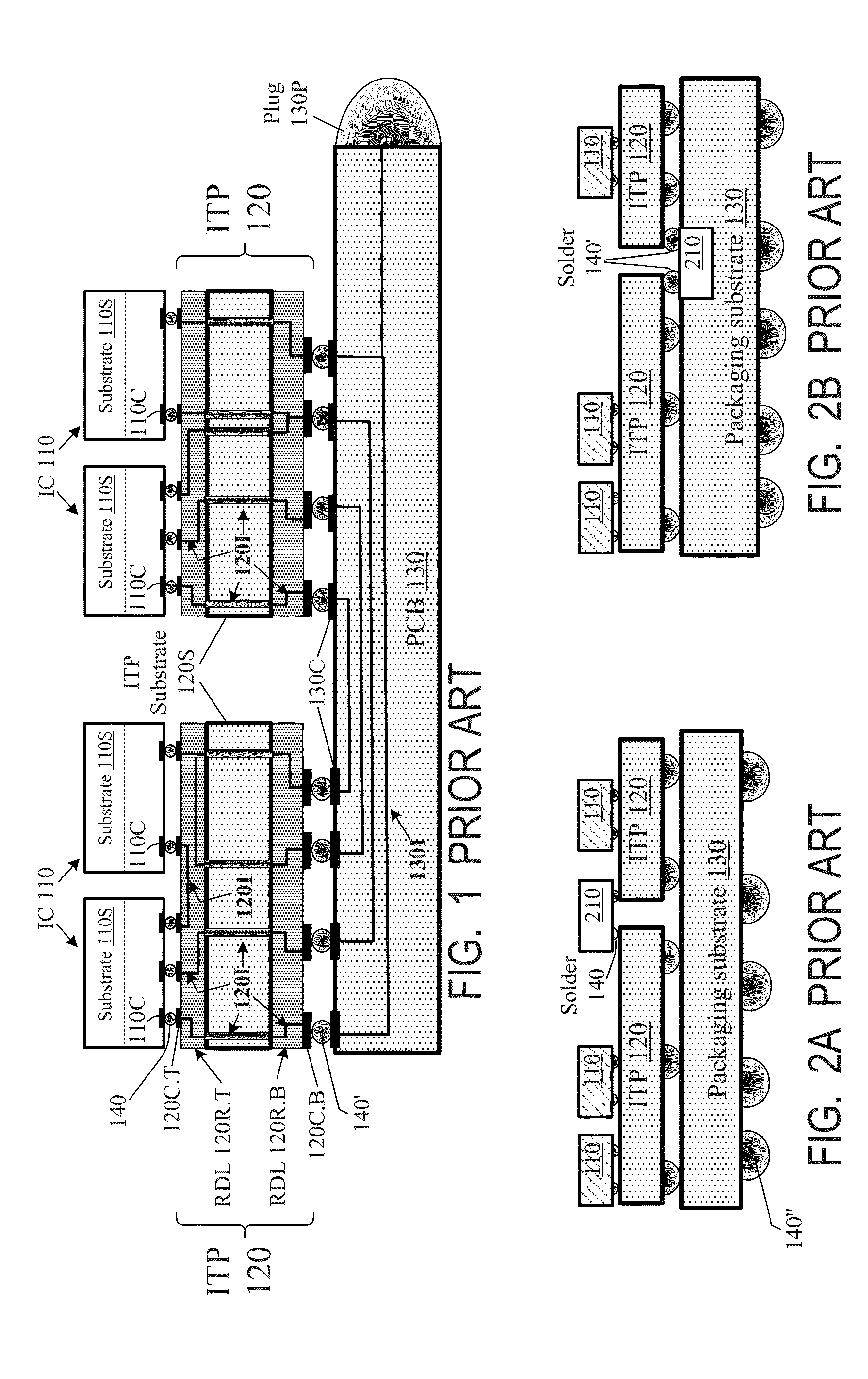
However, use of large interposers leads to large stresses on connections 140 and 140′.
If the interposers 120 are thin and fragile, they can be easily damaged during fabrication, and further it is difficult to keep them flat because they easily warp.
Attaching dies to the interposers is difficult if the interposers are warped and fragile as noted above.

Method used


Image

  • Circuit assemblies with multiple interposer substrates, and methods of fabrication
  • Circuit assemblies with multiple interposer substrates, and methods of fabrication
  • Circuit assemblies with multiple interposer substrates, and methods of fabrication

Examples


Embodiment Construction

[0023]The embodiments described in this section illustrate but do not limit the invention. The invention is defined by the appended claims.

[0024]FIGS. 5A, 5B illustrate beginning stages of interposer fabrication according to some embodiments of the present invention. FIG. 5A shows a vertical cross section marked A-A in the top view of FIG. 5B; FIG. 5B is on a smaller scale than FIG. 5A. A number of interposers will be manufactured based on a common substrate 120S. In FIG. 5B, the interposer substrate 120S is shown as part of a round wafer (could be a silicon wafer for example), but substrate 120S could be of any desired shape and material; exemplary materials include semiconductor materials, metals and other conductors, and dielectrics (organic or inorganic).

[0025]In the example shown, substrate 120S will yield a combined interposer 120 containing seven constituent interposers 120.1, . . . 120.7 whose substrates are shown at 120.1S through 120.7S respectively. Each substrate 120.iS ...


PUM


Abstract

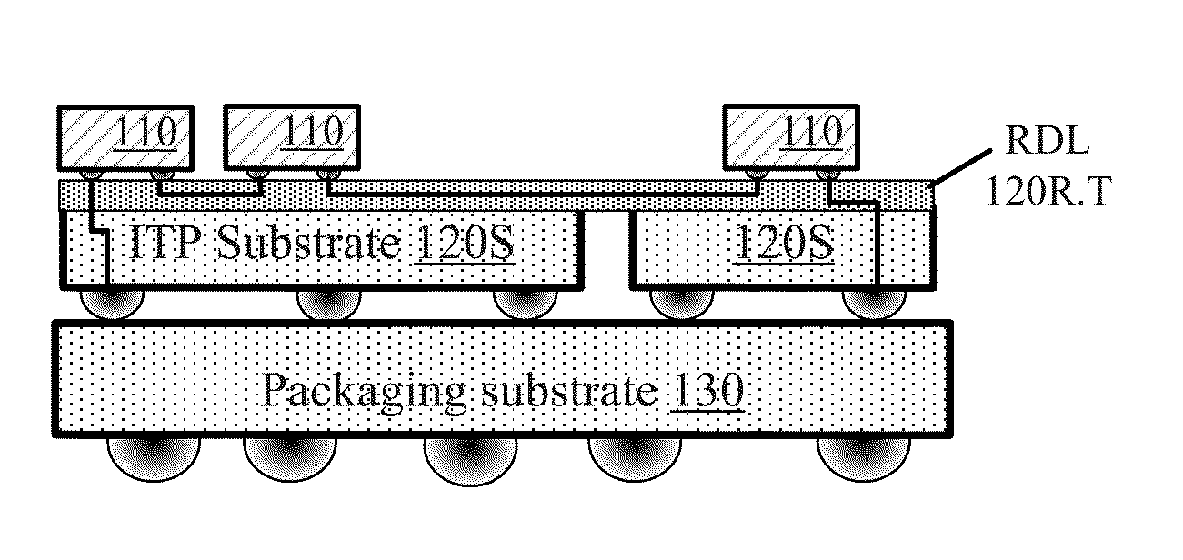
A combined interposer (120) includes multiple constituent interposers (120.i), each with its own substrate (120.iS) and with a circuit layer (e.g. redistribution layer) on top and / or bottom of the substrate. The top circuit layers can be part of a common circuit layer (120R.T) which can interconnect different interposers. Likewise, the bottom circuit layers can be part of a common circuit layer (120R.B). The constituent interposer substrates (120.iS) are initially part of a common wafer, and the common top circuit layer is fabricated before separation of the constituent interposer substrates from the wafer. Use of separated substrates reduces stress compared to use of a single large substrate. Other features are also provided.

Description

BACKGROUND OF THE INVENTION[0001]This document relates to circuit assemblies that include integrated circuits (ICs) and interposers.[0002]A typical IC is a small, fragile device with tiny contact pads that cannot be directly connected to large electro-mechanical connectors such as screw connectors or computer-card slots. Therefore, ICs are packaged into sturdier packages having larger contact pads. The packages should preferably be small and allow circuits to be interconnected by short electrical paths to provide high speed and low power consumption. To achieve these objectives, a single package may interconnect multiple circuits. For example, a package may include a number of ICs and discrete circuits attached to a printed circuit board (PCB) to form a sturdy computer card that can be forced into a tight computer-card slot without breakage. The PCB includes interconnect lines that interconnect multiple ICs or other circuits and connect them to a sturdy plug insertable into the slot...

Claims


Application Information

Patent Timeline
IPC IPC(8): H05K1/11H05K1/14H05K1/18H05K1/02H01L25/065H01L25/00
CPCH05K1/111H01L25/0655H05K1/141H05K1/181H05K1/0271H01L25/50H01L23/5385H01L25/0652H01L2924/181H01L2224/16225H01L2924/15192H01L2924/15311H01L23/3128H01L21/561H01L23/562H01L24/13H01L24/16H01L24/32H01L21/6835H01L24/48H01L24/73H01L24/81H01L24/92H01L24/97H01L25/03H01L2224/0401H01L2224/04042H01L2224/131H01L2224/16227H01L2224/32145H01L2224/48227H01L2224/73204H01L2224/73253H01L2224/81203H01L2224/81801H01L2224/92125H01L2224/97H01L2225/0651H01L2225/06517H01L2225/06589H01L2924/14H01L2924/157H01L2924/1615H01L2924/16153H01L2924/16251H01L2225/06562H01L2221/68327H01L2924/15174H01L2924/00014H01L2924/00012H01L2224/81H01L2224/85H01L2924/014H01L2224/83H01L2224/45099H01L2224/45015H01L2924/207H01L23/498H01L23/538H01L23/5383H01L23/5389H01L23/5381H01L21/76898H01L21/4853H01L21/486H01L21/56H01L23/3121H01L23/49827H01L23/49833H01L23/49838H01L24/17
Inventor SHEN, HONGSUN, ZHUOWENWOYCHIK, CHARLES G.SITARAM, ARKALGUD
Owner INVENSAS CORP
Learn More