Image sensing circuit and method capable of obtaining higher image brightness dynamic range
- Summary
- Abstract
- Description
- Claims
- Application Information
AI Technical Summary
Benefits of technology
Problems solved by technology
Method used
Image

Examples
first embodiment
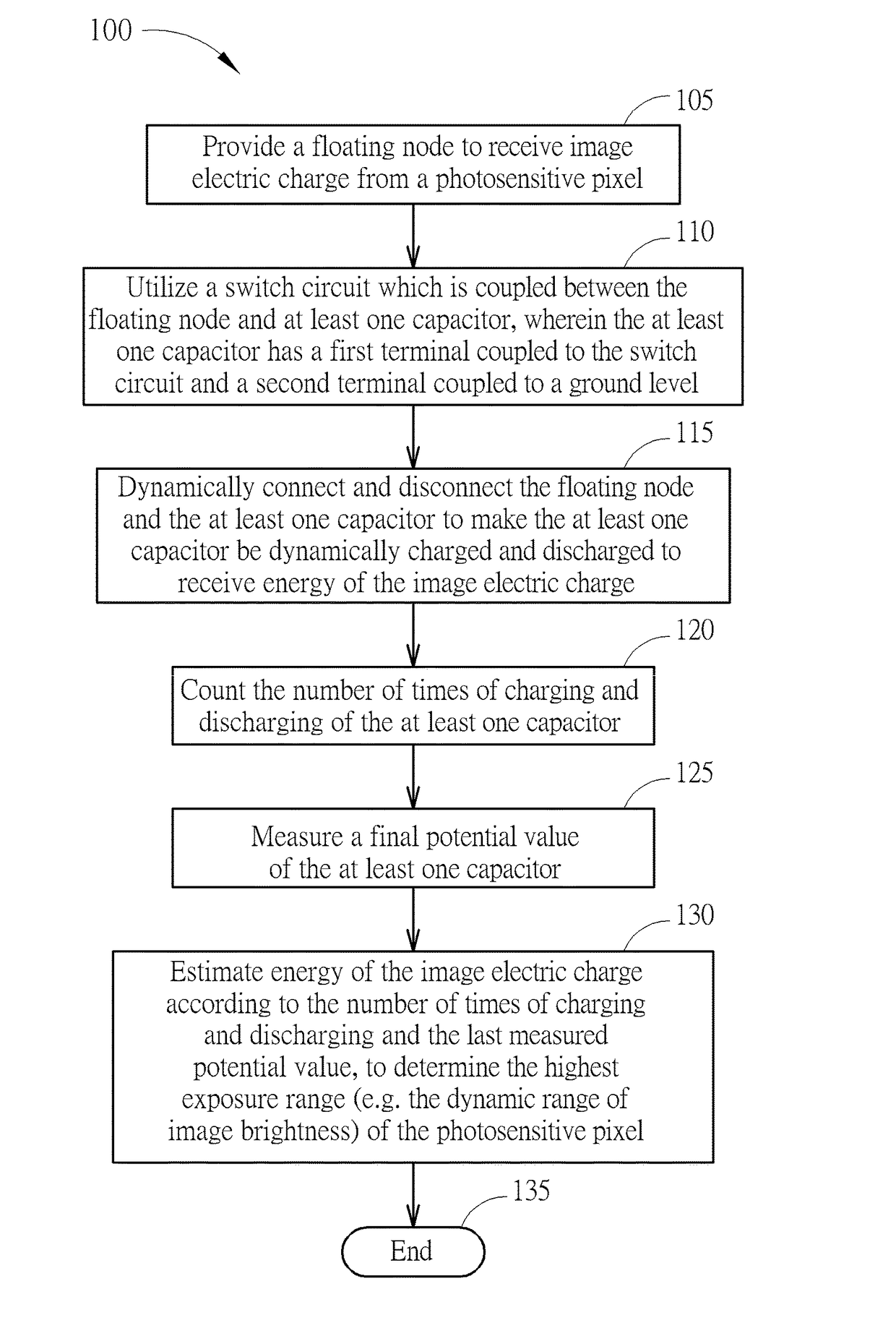
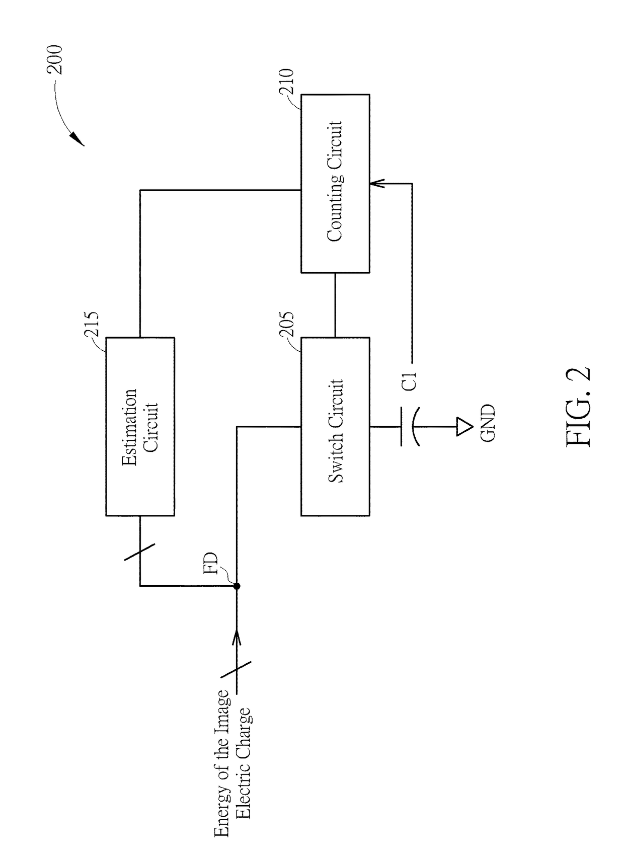
[0018]Furthermore, in an alternative design of the first embodiment, the estimation circuit 215 is implemented outside the image sensing circuit 200 and thus excluded from the image sensing circuit 200. In other words, the image sensing circuit 200 is arranged to control and count a number of times of charging and discharging the capacitor C1, and the subsequent estimation operation is performed by an external estimation circuit. In addition, the switch circuit 205 and the counting circuit 210 may be integrated into a same circuit.
[0019]A second embodiment of the present invention is to utilize two capacitors which are sequentially charged and discharged to replace / simulate a single capacitor, and estimate / determine a potential difference increment (or voltage increment) correspondingly generated by the energy of image electric charge through monitoring the charging and discharging behavior of the two capacitors, so as to equivalently judge the amount of the energy of image electric...
second embodiment
[0022]Furthermore, in an alternative design of the second embodiment, the estimation circuit 315 may be implemented outside the image sensing circuit 300 and thus excluded from the image sensing circuit 300. In other words, the image sensing circuit 300 is arranged to control and count a number of times of charging and discharging the capacitor C1 and a number of times of charging and discharging the capacitor C2, and the subsequent estimation operation is performed by an external estimation circuit. In addition, the switch circuit 305 and the counting circuit 310 may be integrated into a same circuit. Moreover, the capacitors C1 and C2 may be implemented with capacitors having the same capacitance value or capacitors having different capacitance values. If the capacitors C1 and C2 are implemented with capacitors having different capacitance values, the estimation circuit 315 must refer to the different capacitance values of the capacitors C1 and C2, the judged respective potential ...
third embodiment
[0023]Moreover, the operation of sequentially charging and discharging two capacitors in the present invention may be implemented with an automated control mechanism. Please refer to FIG. 4, which is a diagram illustrating an image sensing circuit 400 according to the present invention. The image sensing circuit 400 is capable of estimating energy of image electric charge of a photosensitive pixel (which is located outside the image sensing circuit 400 and not shown in FIG. 4). The photosensitive pixel means a pixel unit of a photosensitive element. The pixel unit may generate different amounts of energy of image electric charge in different light source environments (different exposure environments). The image sensing circuit 400 of the present invention can precisely estimate an amount of energy of image electric charge generated by the photosensitive pixel, and correctly calculate an image brightness dynamic range. The image sensing circuit 400 of the present invention is suitabl...
PUM
 Abstract
Description
Claims
Application Information
 - Generate Ideas
- Intellectual Property
- Life Sciences
- Materials
- Tech Scout
- Unparalleled Data Quality
- Higher Quality Content
- 60% Fewer Hallucinations
Browse by: Latest US Patents, China's latest patents, Technical Efficacy Thesaurus, Application Domain, Technology Topic, Popular Technical Reports.
© 2025 PatSnap. All rights reserved.Legal|Privacy policy|Modern Slavery Act Transparency Statement|Sitemap|About US| Contact US: help@patsnap.com