Imprint apparatus and method of manufacturing article
a technology of printing apparatus and manufacturing method, which is applied in the direction of photomechanical apparatus, instruments, coatings, etc., can solve the problems of clogging of the discharge outlet for discharging imprint material, defect of pattern formation, and lack of part of the imprint material to be supplied onto the substrate, etc., and achieve the effect of correcting pattern formation
- Summary
- Abstract
- Description
- Claims
- Application Information
AI Technical Summary
Benefits of technology
Problems solved by technology
Method used
Image
Examples
first embodiment
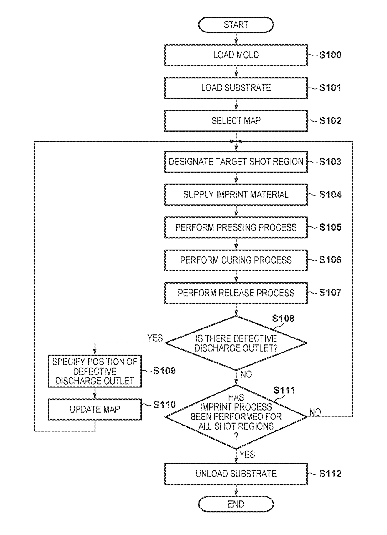
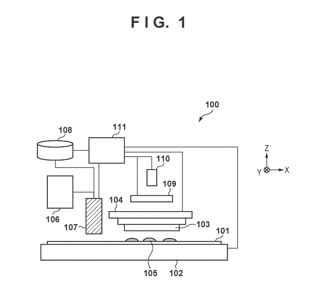
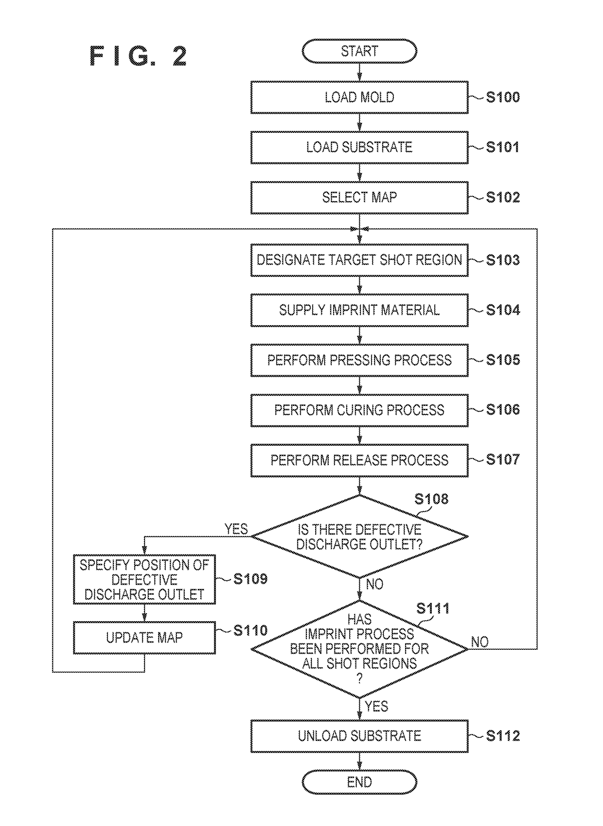
[0022]FIG. 1 is a schematic view showing the arrangement of an imprint apparatus 100 according to one aspect of the present invention. The imprint apparatus 100 is a lithography apparatus used in a process of manufacturing a semiconductor device or the like. The imprint apparatus 100 performs an imprint process of forming a pattern by molding an imprint material on a substrate.
[0023]This embodiment assumes a photocuring resin material as an imprint material, and adopts a photocuring method of curing the imprint material by irradiation with light (ultraviolet light or the like). However, the present invention does not limit the imprint material to the resin material, and may use, for example, a photocuring material including a powder or particles of an inorganic material. In addition, the present invention does not limit the imprint material curing method to the photocuring method, and may adopt, for example, a heat-curing method of curing an imprint material by heat.
[0024]As shown i...
second embodiment
[0067]Update (step S110) of a map according to the second embodiment will be described in detail. FIGS. 7A and 7B are views each showing the relationship between the plurality of discharge outlets of a discharge unit 107 and a map (coordinate data about the supply positions of droplets of an imprint material 105). The discharge unit 107 includes, as the plurality of discharge outlets, 16 discharge outlets a1 to a16 arrayed in the Y-axis direction. In this embodiment, the imprint material 105 is supplied onto a substrate as follows. First, a substrate 101 is scanned in the X-axis (+) direction (forward path) while discharging droplets of the imprint material 105 from the discharge outlets a1 to a16. Next, discharge of droplets of the imprint material 105 from the discharge outlets a1 to a16 is stopped, and the substrate 101 is shifted in the Y-axis direction by a distance corresponding to half the interval between the discharge outlets a1 to a16. Then, the substrate 101 is scanned in...
third embodiment
[0074]Update (step S110) of a map according to the third embodiment will be described in detail. FIGS. 8A and 8B are views each showing the relationship between the plurality of discharge outlets of a discharge unit 107 and a map (coordinate data about the supply positions of droplets of an imprint material 105). The arrangement of the discharge unit 107 and supply of the imprint material 105 onto a substrate are the same as in the second embodiment.
[0075]In this embodiment, assume that a concave-convex pattern of a predetermined period, that is, a plurality of line patterns (line-and-space pattern) are formed on a mold 103 in the Y-axis direction. When the mold 103 on which the line patterns have been formed and the imprint material 105 on the substrate are brought into contact with each other, the filling speed of the imprint material 105 generally tends to increase in a direction along the line patterns, and decrease in a direction orthogonal to the direction along the line patte...
PUM
| Property | Measurement | Unit |
|---|---|---|
| intersecting angle | aaaaa | aaaaa |
| time | aaaaa | aaaaa |
| distance | aaaaa | aaaaa |
Abstract
Description
Claims
Application Information


