Electronic component-embedded board and electronic component device
- Summary
- Abstract
- Description
- Claims
- Application Information
AI Technical Summary
Benefits of technology
Problems solved by technology
Method used
Image

Examples
embodiment
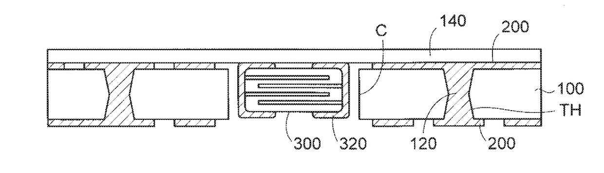
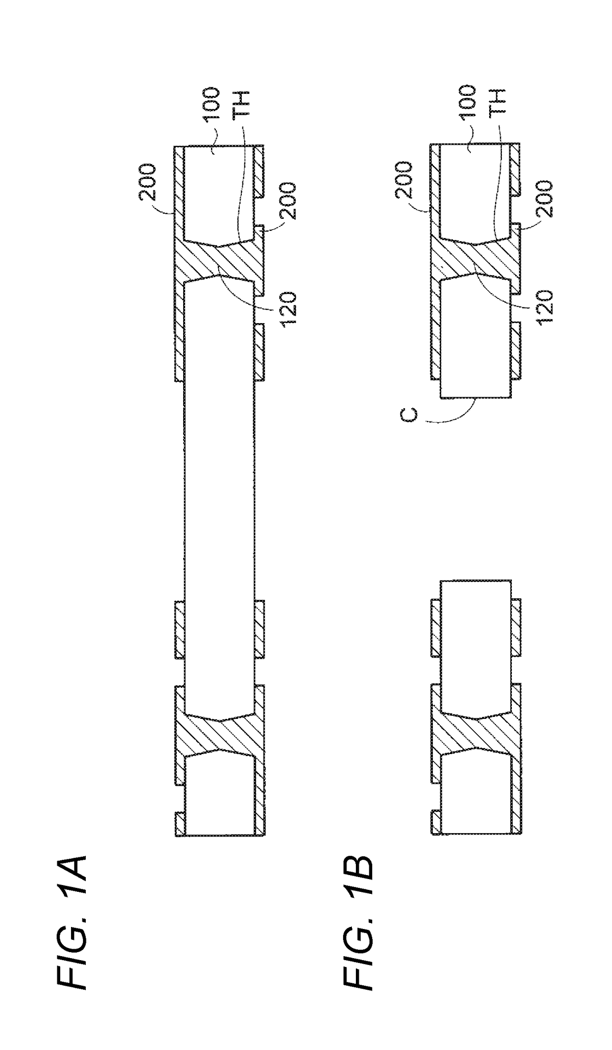
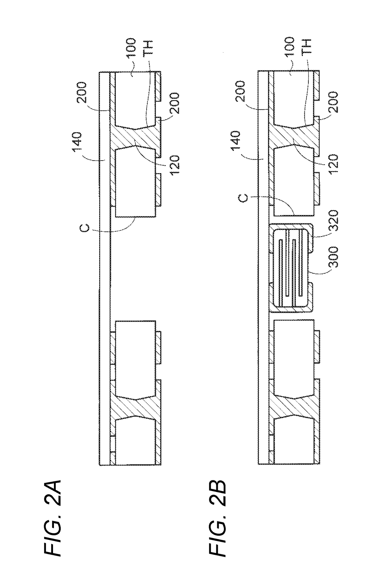
[0091]FIGS. 8 to 17 are views for explaining a manufacturing method for the electronic component-embedded board according to the embodiment. FIGS. 18 and 19 are views illustrating the electronic component-embedded board according to the embodiment. The structure of the electronic component-embedded board and the structure of an electronic component device will be described below in parallel with description of the manufacturing method for the electronic component-embedded board.
[0092]In the manufacturing method for the electronic component-embedded board according to the embodiment, first, a core substrate 10 having a structure illustrated in FIGS. 8A and 8B is prepared. The core substrate 10 is formed of an insulating material such as glass cloth impregnated with an epoxy resin.
[0093]First wiring layers 20 are formed respectively on two face sides of the core substrate 10. Through holes TH are formed to penetrate the core substrate 10 in a thickness direction. The first wiring laye...
PUM
 Abstract
Description
Claims
Application Information
 - R&D Engineer
- R&D Manager
- IP Professional
- Industry Leading Data Capabilities
- Powerful AI technology
- Patent DNA Extraction
Browse by: Latest US Patents, China's latest patents, Technical Efficacy Thesaurus, Application Domain, Technology Topic.
© 2024 PatSnap. All rights reserved.Legal|Privacy policy|Modern Slavery Act Transparency Statement|Sitemap