OLED touch display device

a technology of touch display and light-emitting diodes, which is applied in semiconductor devices, instruments, computing, etc., can solve the problems of reducing display quality, reducing display area, and difficulty in routing the number of traces between the touch sense electrode and the touch control circuit, so as to reduce the number of traces, save layout area, and reduce manufacturing cost

Inactive Publication Date: 2018-10-25
SUPERC TOUCH CORP
View PDF5 Cites 14 Cited by
  • Summary
  • Abstract
  • Description
  • Claims
  • Application Information

AI Technical Summary

Benefits of technology

[0007]The object of the present invention is to provide an OLED touch display device capable of greatly reducing the number of traces, significantly saving layout area and reducing the manufacturing cost in comparison with the prior art.

Problems solved by technology

With the large number of traces, it is difficult to route the number of traces between the touch sense electrodes and the touch control circuit.
Moreover, the layout of the traces may occupy a lot of area, resulting in reducing the display area and lowering the display quality.

Method used


Image

  • OLED touch display device
  • OLED touch display device
  • OLED touch display device

Examples


Embodiment Construction

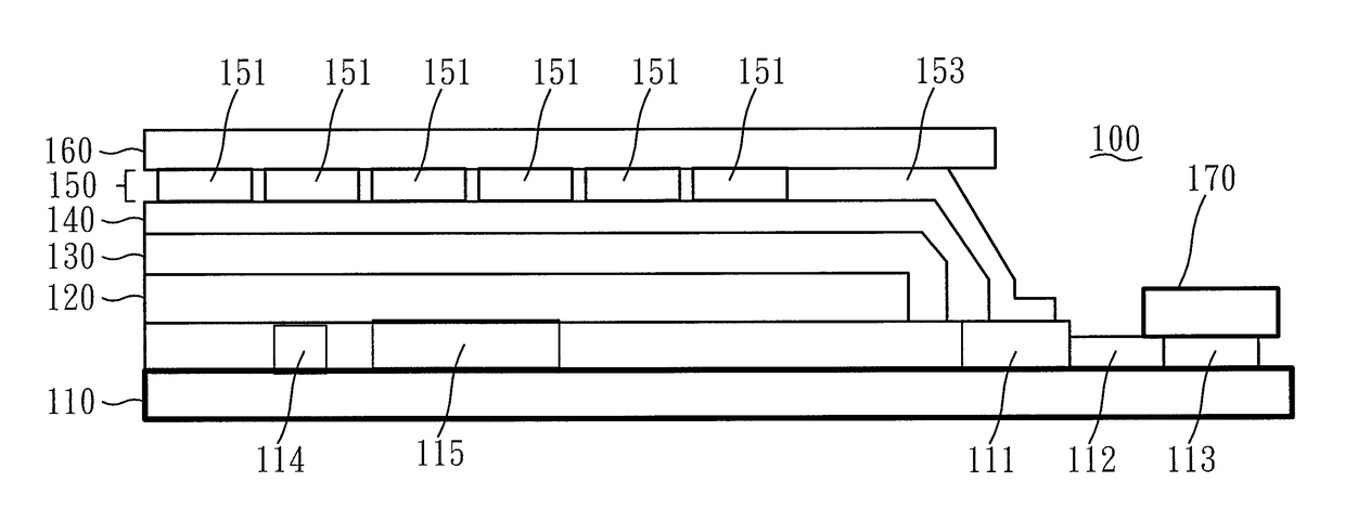
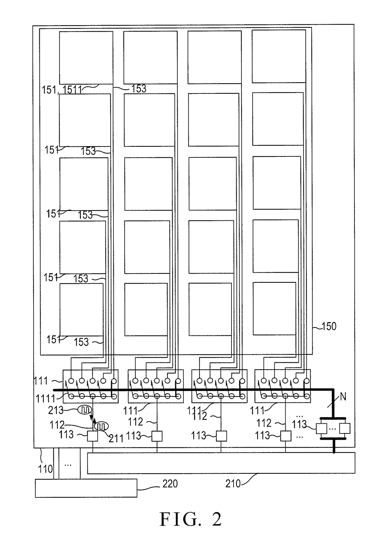
[0025]The present invention relates to an OLED touch display device. FIG. 1 is a first exemplary stack-up diagram of the OLED touch display device 100 in accordance with the present disclosure. As shown, the OLED touch display device 100 includes a thin film transistor (TFT) substrate 110, an OLED layer 120, a common voltage electrode layer 130, an encapsulation layer 140, at least one touch electrode layer 150, and a touch protective layer 160.

[0026]The TFT substrate 110 has a surface formed thereon a plurality of switch devices 111, a plurality of second touch traces 112, a plurality of conductive pads 113, a plurality of display thin film transistors 114, a plurality of display pixel electrodes 115, a plurality of gate lines (not shown), and a plurality of data lines (not shown). The material of the TFT substrate 110 can be selected from the group consisting of: polyethylene terephthalate (PET), polyimide (PI), polycarbonate (PC), cyclo-olefin polymers (COP), Poly methyl methacry...


PUM


Abstract

An OLED touch display device includes a TFT substrate and a touch electrode layer. The TFT substrate has a surface formed thereon plural switch devices, plural second touch traces and plural conductive pads. Each switch device has plural touch TFT switches. The touch electrode layer includes plural first touch traces and plural touch sense electrodes divided into plural groups each having at least one touch sense electrode, and each group is corresponding to one of the conductive pads. The touch sense electrodes are corresponding to the first touch traces one by on. Each touch sense electrode is connected to the corresponding first touch trace. Each first touch trace is connected to one touch TFT switch of the corresponding switch device, and each switch device is connected to one second touch trace and the corresponding conductive pad.

Description

BACKGROUND OF THE INVENTION1. Field of the Invention[0001]The present invention relates to a touch display panel and, more particularly, to an organic light emitting diode display (OLED) touch display device.2. Description of Related Art[0002]In recent years, the flat panel display industry has been rapidly developed, and many products have also been made in pursuit of light weight, thinness, small volume and fine image quality for developing several types of flat panel displays to replace traditional cathode ray tube display (CRT). The flat panel display includes liquid crystal display (LCD), plasma display panel (PDP), organic light emitting diode (OLED) display, field emission display (FED), and vacuum fluorescence display (VFD).[0003]Among these types of flat panel displays, the organic light emitting diode display (OLED) technology is the one with great potential. The OLED display is provided with not only the advantages of LCD display including thinness, power-saving and full-...

Claims


Application Information

Patent Timeline
Patent Type & Authority Applications(United States)
IPC IPC(8): H01L27/32G06F3/041G06F3/044
CPCH01L27/323G06F3/0412G06F3/0416G06F2203/04104H01L27/3262H01L27/3276G06F2203/04112G06F3/044H10K59/40H10K59/12H10K59/131G06F3/0446G06F3/0445G06F3/04164H10K59/1213
Inventor LEE, HSIANG-YUCHIN, SHANGLIN, PING-TSUNTU, CHIA-HSUN
Owner SUPERC TOUCH CORP
Why Eureka
Try Eureka