TFT circuit and shift register circuit
a shift register and circuit technology, applied in the field of tft circuits, can solve the problems of generating flickering based on residual charge, deteriorating display quality, and not being able to immediately clear substrates,
- Summary
- Abstract
- Description
- Claims
- Application Information
AI Technical Summary
Benefits of technology
Problems solved by technology
Method used
Image

Examples
first embodiment
[0038]A description will be given of a first embodiment of a TFT circuit according to the present invention with reference to the drawings. It is only necessary that the TFT circuit of the present embodiment includes a plurality of depression-type TFTs and the TFT circuit of the present embodiment may be a drive circuit such as a gate driver. All of the TFTs included in the TFT circuit may be depression-type or only some of the TFTs may be depression-type. A description will be given below of a TFT circuit using an n-channel TFT as a depression-type TFT.
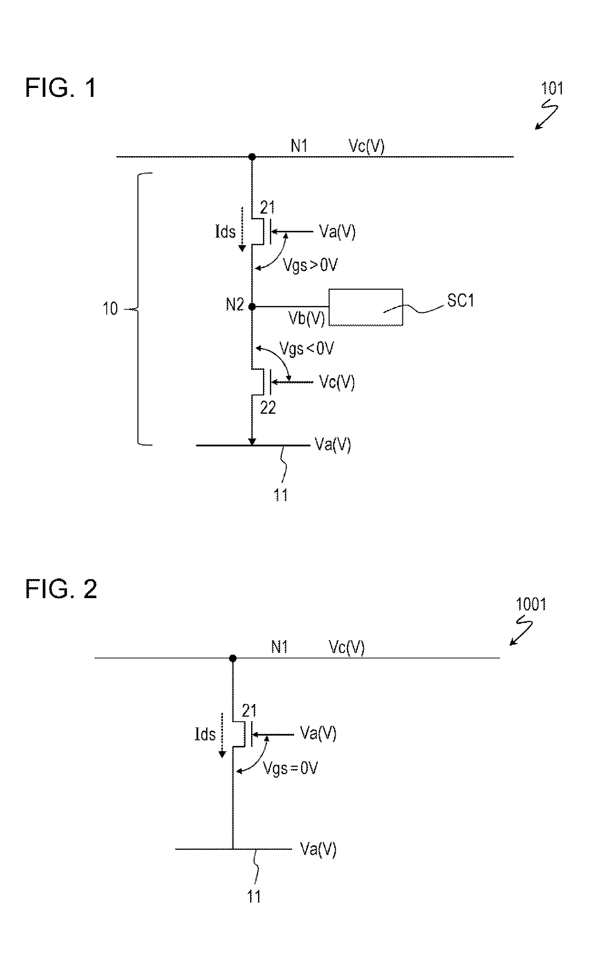
[0039]FIG. 1 is a diagram schematically illustrating part of the TFT circuit of the present embodiment.
[0040]The TFT circuit 101 has a first node N1 to which a first low potential Vc is supplied, a depression-type first TFT 21 arranged between the first node N1 and low-potential wiring 11, and a depression-type second TFT 22 arranged between the first TFT 21 and the low-potential wiring 11. The low-potential wiring 11 is wiring for s...
second embodiment
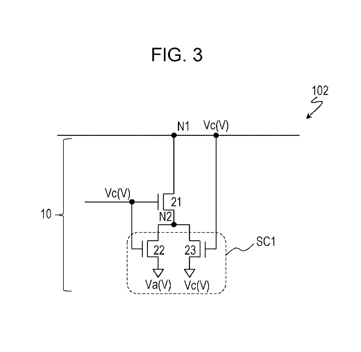
[0049]FIG. 3 is a diagram illustrating part of a TFT circuit 102 of the second embodiment. In FIG. 3, the same reference numerals are attached to similar constituent components to those in FIG. 1, and a description thereof will be omitted.
[0050]The TFT circuit 102 is provided with the first node N1 to which the first low potential Vc is supplied, the first TFT 21 connected to the first node N1, and the second TFT 22 arranged between the first TFT 21 and the low-potential wiring which supplies a second low potential Va. For example, the first low potential Vc is supplied to the gate terminals of the first TFT 21 and the second TFT 22. The second node N2 which may enter a floating state is formed between the source terminal of the first TFT 21 and the source terminal of the second TFT 22. A depression-type third TFT 23 is connected to the second node N2.
[0051]Also, in the present embodiment, similarly to the first embodiment, the sub-circuit SC1 capable of supplying the third low pote...
application example 1
to Shift Register Circuit
[0054]The present embodiment is able to be applied to, for example, a shift register circuit forming a monolithic gate driver. A description will be given below of an example in which the present embodiment is applied to a shift register circuit.
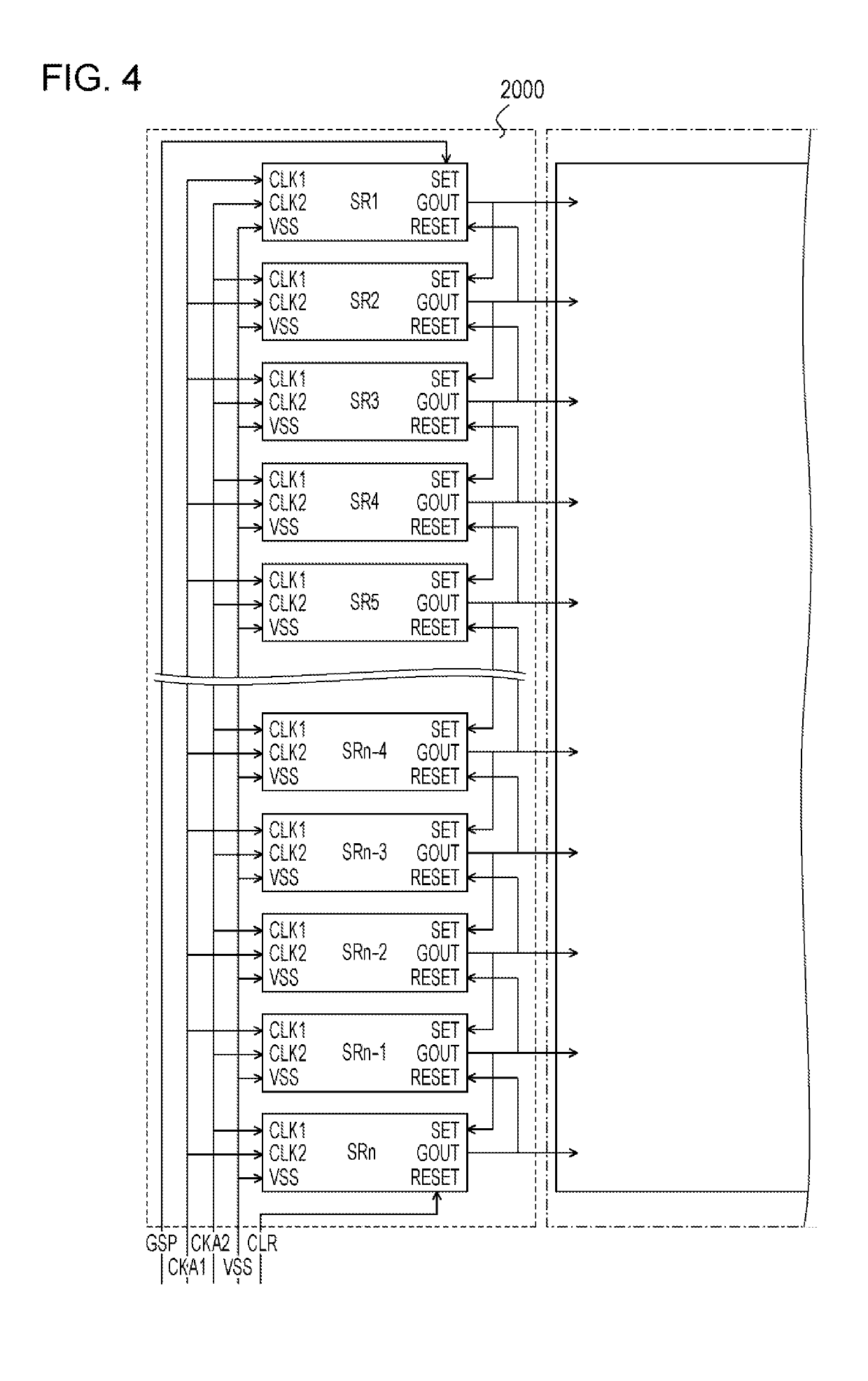
[0055]First, referring to FIG. 4, a configuration of a shift register circuit 2000 of the related art is illustrated as Reference Example 1. The configuration thereof is disclosed, for example, in International Publication No. 2011 / 135879.
[0056]The shift register circuit 2000 has a plurality of unit circuits (hereinafter referred to as “unit circuits”) SR1 to SRn. A unit terminal SRk (k is a natural number of 1≤k≤n) of each stage is provided with a set terminal for inputting a set signal SET, an output terminal for outputting an output signal GOUT, a reset terminal for inputting a reset signal RESET, a low power supply input terminal for inputting a low power supply potential VSS, and a clock input terminal for input...
PUM
 Abstract
Description
Claims
Application Information
 - R&D Engineer
- R&D Manager
- IP Professional
- Industry Leading Data Capabilities
- Powerful AI technology
- Patent DNA Extraction
Browse by: Latest US Patents, China's latest patents, Technical Efficacy Thesaurus, Application Domain, Technology Topic.
© 2024 PatSnap. All rights reserved.Legal|Privacy policy|Modern Slavery Act Transparency Statement|Sitemap