Method of manufacturing organic el display panel, organic el display panel, and organic el display device

a technology of organic el and display panels, which is applied in the direction of organic semiconductor devices, solid-state devices, semiconductor devices, etc., can solve problems such as panel defects

Active Publication Date: 2019-07-18
JOLED INC
View PDF0 Cites 6 Cited by
  • Summary
  • Abstract
  • Description
  • Claims
  • Application Information

AI Technical Summary

Problems solved by technology

Mixing, due to ink including functional material overflowing banks, particularly in the case of ink including lig

Method used


Image

  • Method of manufacturing organic el display panel, organic el display panel, and organic el display device
  • Method of manufacturing organic el display panel, organic el display panel, and organic el display device
  • Method of manufacturing organic el display panel, organic el display panel, and organic el display device

Examples


embodiment 1

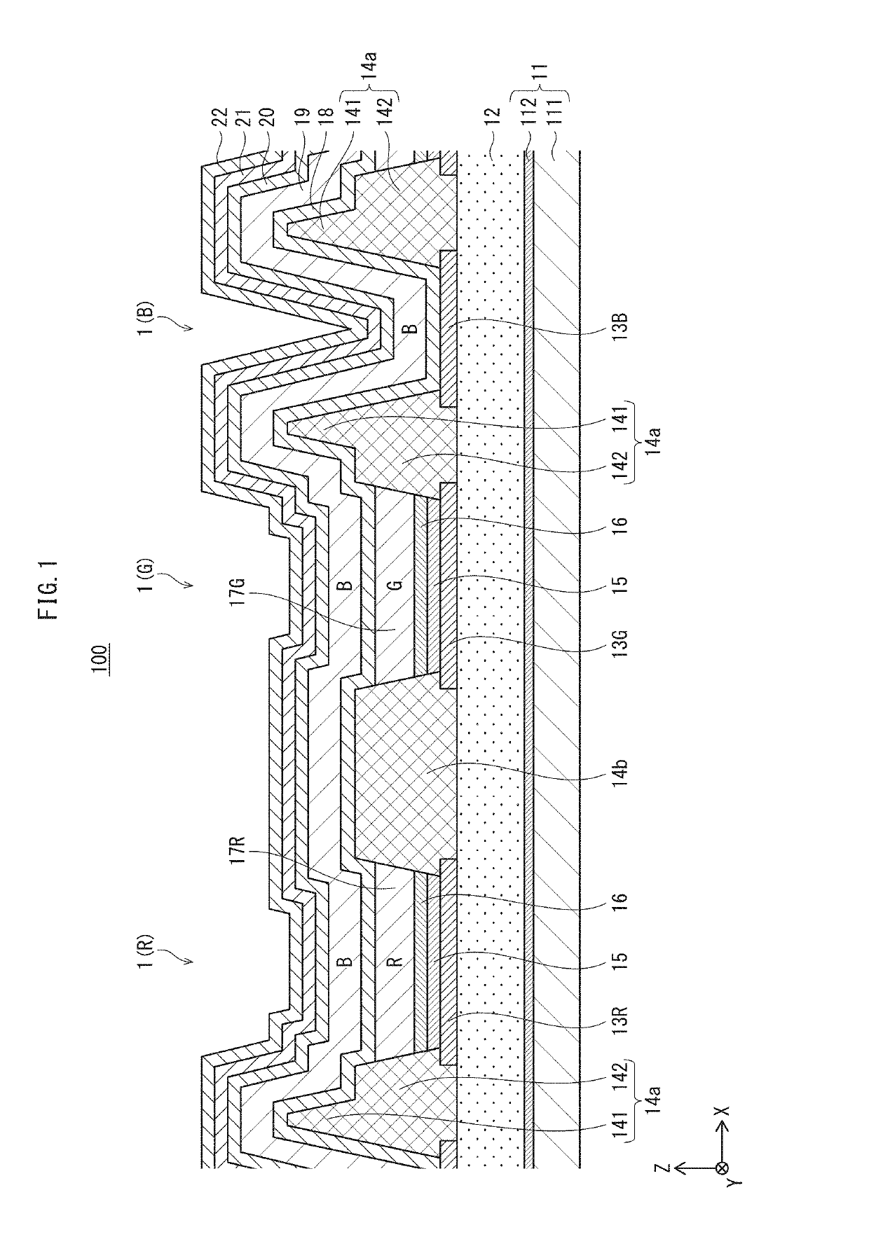
[0063]FIG. 1 is a cross section diagram of a portion of an organic EL display panel 100 (see FIG. 10) pertaining to The organic EL display panel 100 includes pixels, each pixel including organic EL elements 1(R), 1(G), 1(B) that emit red light, green light, and blue light, respectively. In FIG. 1, a cross section of one such pixel is illustrated.

[0064]In the organic EL display panel 100, each organic EL element 1 is a top-emission type that emits light in a forwards direction (away from the substrate).

[0065]The organic EL element 1(R) and the organic EL element 1(G) have substantially the same structure, and therefore are described as the organic EL element 1(R / G) unless a distinction is made. Further, portions of the organic EL element 1(R / G) and the organic EL element 1(B) that have similar structure may be described the organic EL element 1 where a distinction is not made.

[0066]As illustrated in FIG. 1, the organic EL element 1(R / G) includes a substrate 11, an interlayer insulat...


PUM


Abstract

In a method for manufacturing an organic EL display panel including: preparing a substrate; forming pixel electrodes in a matrix of rows and columns; forming banks extending in a column direction at least between the pixel electrodes in a row direction; forming a first light emitting layer by applying an ink including a light emitting material in a first gap selected from a plurality of gaps between the banks; forming a second light emitting layer by a vapor deposition method to be continuous above both the first light emitting layer and the pixel electrodes in a second gap adjacent in the row direction to the first gap; and forming a counter electrode above the second light emitting layer, a height of portions of the banks adjacent to the second gap is made to be greater than a height of portions of the banks adjacent to the first gap.

Description

[0001]This application claims priority to Japanese Patent Application No. 2018-004121, filed Jan. 15, 2018, the contents of which are hereby incorporated by reference in their entirety.BACKGROUNDTechnical Field[0002]The present disclosure relates to methods of manufacturing organic electroluminescence (EL) display panels that include organic EL elements that make use of electroluminescence of organic materials, organic EL display panels, and organic EL display devices that make use of organic EL display panels.Description of Related Art[0003]In recent years, use of organic EL elements in display devices is becoming widespread.[0004]Organic EL elements have a structure in which at least a light emitting layer is sandwiched between an anode and a cathode. A method by which ink including an organic functional material is applied by a wet process such as inkjet application is known as a method of efficiently forming light emitting layers and functional layers. It is possible to use a sm...

Claims


Application Information

Patent Timeline
IPC IPC(8): H01L27/32H01L51/56H01L51/00H01L51/50
CPCH01L27/3246H01L51/56H01L51/0021H01L51/0005H01L51/0008H01L27/3211H01L51/504H01L27/322H01L51/5218H01L51/5234H01L2227/323H01L51/5209H01L51/5253H01L2251/5315H10K59/35H10K59/122H10K71/135H10K71/16H10K50/131H10K71/00H10K71/166H10K50/813H10K2102/351H10K50/13H10K59/38H10K71/60H10K50/00H10K50/80H10K50/818H10K50/828H10K50/844H10K59/1201H10K2102/3026
Inventor KAMIYAMA, ISAO
Owner JOLED INC
Why Eureka
Try Eureka