

Electronic device
- Summary
- Abstract
- Description
- Claims
- Application Information
AI Technical Summary
Benefits of technology
Problems solved by technology
Method used
Image


Examples
Embodiment Construction
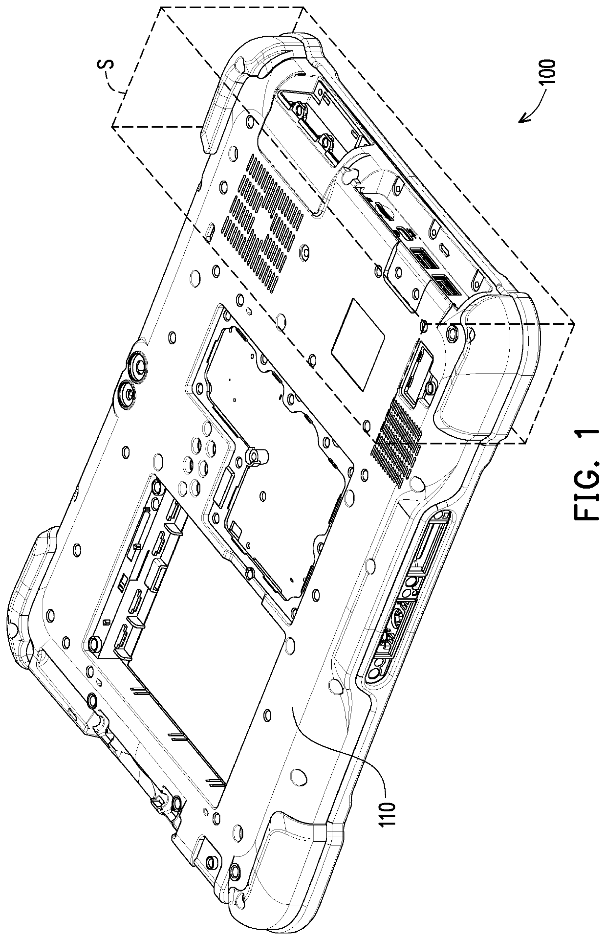
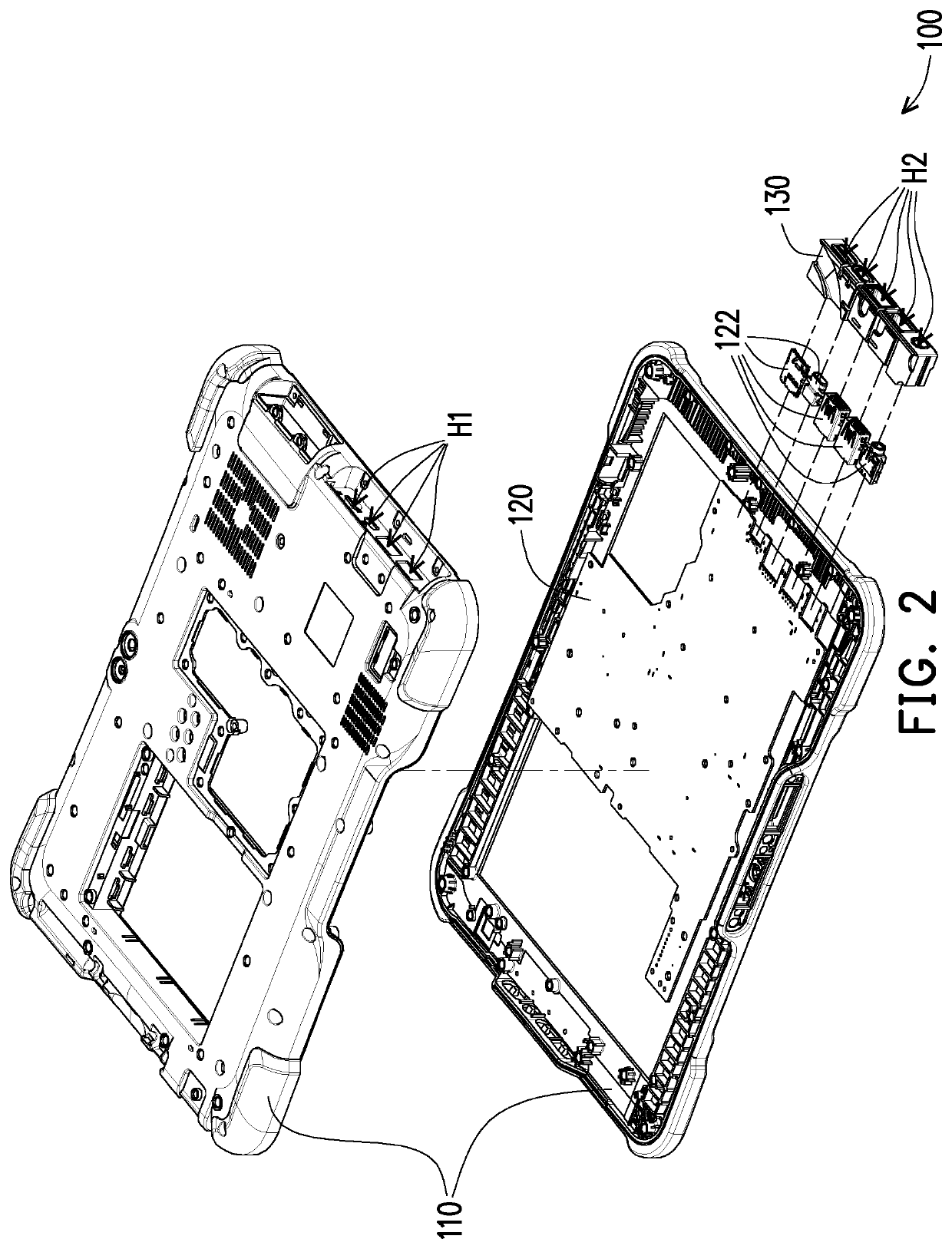
[0025]FIG. 1 is a three-dimensional schematic diagram of an electronic device according to one embodiment of the present invention. FIG. 2 is an exploded view of the electronic device of FIG. 1. FIG. 3A and FIG. 3B are respective local cross-section views at different viewing angles of the electronic device of FIG. 1. Referring to FIG. 1 to FIG. 3B, an electronic device 100 of the present embodiment includes a casing 110, at least one connector 122 and a waterproof elastic module 130. The casing 110 includes at least one first hole H1 formed at a side S of the casing 110. The at least one connector 122 is disposed in the casing 110, the at least one connector 122 penetrates the at least one first hole H1 and is exposed out of the at least one first hole H1, and at least one gap G exists between the plurality of walls 112 of the casing 110 encircling the at least one first hole H1 and the corresponding at least one connector 122. The waterproof elastic module 130 has at least one sec...
PUM
 Abstract
Description
Claims
Application Information