
Waveguide manufacturing process
a manufacturing process and waveguide technology, applied in the field of optoelectronics, can solve the problems of diffusion loss, non-linear effect loss, mainly diffuse loss, etc., and achieve the effect of reducing the roughness of the waveguide flanks, low optical loss, and reducing the absorption loss of the waveguide manufactured by the method according to the invention
- Summary
- Abstract
- Description
- Claims
- Application Information
AI Technical Summary
Benefits of technology
Problems solved by technology
Method used
Image

Examples
first embodiment
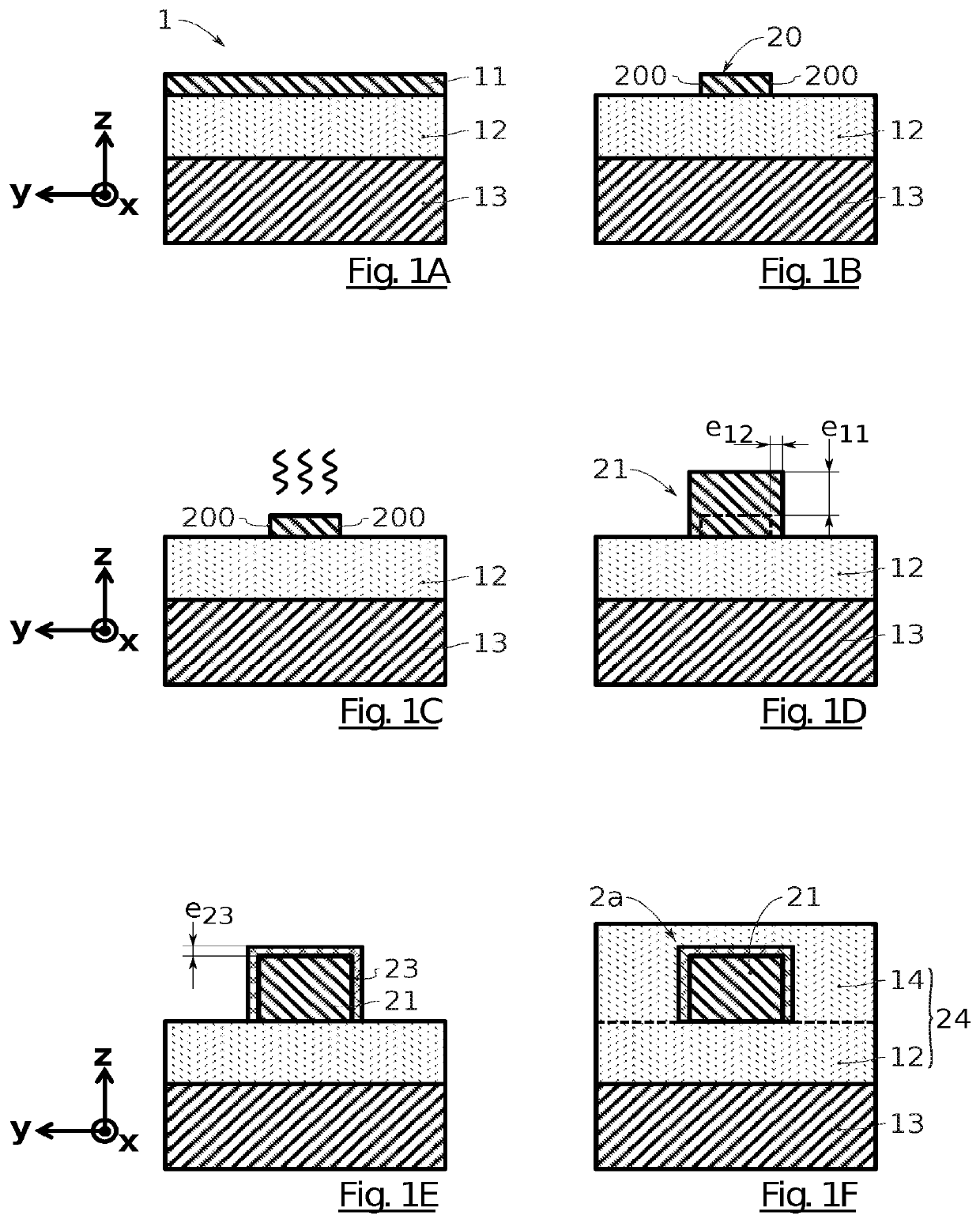
[0072]Preferably, an encapsulation of the core is then carried out by an encapsulation layer 14 (FIG. 1F). This encapsulation layer 14 is preferably made of SiO2. It can be deposited via CVD. It makes it possible to form another portion of the clad of the waveguide. The clad 24 is thus formed all around the core by the layers 12 and 14 made of SiO2. This first embodiment makes it possible to form a strip waveguide 2a.
[0073]In order to form a strip waveguide 2a that is single-mode at the wavelengths used in telecommunications (for example about 1.55 μm), the core 21 can have a height along z comprised between 0.2 μm and 0.4 μm, and a width along y comprised between 0.2 μm and 0.4 μm. The lower portion of the clad 24 formed by the layer 12 preferably has a height greater than or equal to 0.7 μm in a single-mode waveguide 2a configuration.
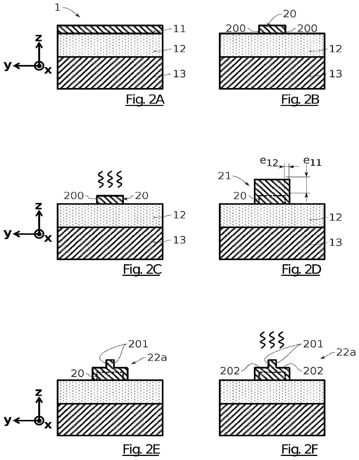
[0074]Other embodiments of the method according to the present invention can be considered. These embodiments can typically combine several sequence...
second embodiment
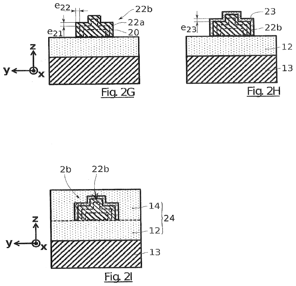
[0081]This second embodiment makes it possible to form an edge waveguide 2b.
[0082]The waveguides manufactured by the method according to the present invention can advantageously be used for LiDAR and 400G long-distance telecom applications, and for quantum photonics and frequency comb applications.
[0083]The invention is not limited to the embodiments described hereinabove and extends to all the embodiments covered by the claims.
[0084]In particular, several steps of etching and / or smoothing and / or epitaxy can be implemented to form the waveguide. In this case, the etching depths and / or the epitaxial thicknesses can vary from one step to another.
PUM
| Property | Measurement | Unit |
|---|---|---|
| thickness | aaaaa | aaaaa |
| epitaxial thickness | aaaaa | aaaaa |
| thickness | aaaaa | aaaaa |
Abstract
Description
Claims
Application Information