
Display device using organic electroluminescent elements

a technology of electroluminescent elements and display devices, which is applied in the direction of discharge tubes, luminescent screens, instruments, etc., can solve the problems of large cooling fans, light loss of power, and high heat generated by light sources

Inactive Publication Date: 2001-07-10
TOYOTA CENT RES & DEV LAB INC
View PDF14 Cites 243 Cited by
  • Summary
  • Abstract
  • Description
  • Claims
  • Application Information

AI Technical Summary

Problems solved by technology

Incidentally, in the display mentioned above, light loses its power greatly when it passes through the liquid crystal panel.
A high voltage needs to be used for the light source, and in this case, there is a problem that high heat is generated by the light source.
To this end, it is necessary to provide the light source with a large reflector, which is a hindrance to the movement toward weight and size reductions of the device itself.
Another problem is the need to provide a large cooling fan for the light source.
Those problems with the projector type display have been obstacles to the widespread use of HUD.
In the liquid crystal displays, which are not spontaneous luminescent type displays, the angle of field can be narrowed easily, but ther

Method used


Image

  • Display device using organic electroluminescent elements
  • Display device using organic electroluminescent elements
  • Display device using organic electroluminescent elements

Examples


Embodiment Construction

An embodiment of the present invention will be described with reference to the accompanying drawings.

[Structure of the Organic EL Panel]

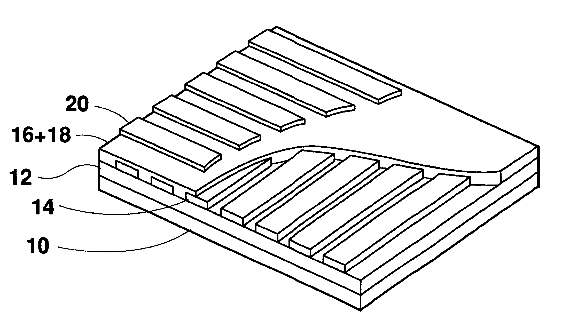
FIG. 1 is a diagram showing the structure of an example of an organic EL panel according to a preferred embodiment of the present invention. The basic structure of a piece of electroluminescent element is the same as in Japanese Patent Laid-Open Publication No. Hei-9-180883. This element is organized by forming a dielectric mirror 12, a transparent electrode 14, a hole transport layer 16, a luminous layer 18, and a metal electrode 20 in this order on a glass substrate.

The glass substrate 10 is in a rectangular form with two 2.5-inch diagonal lines. The dielectric mirror 12 is obtained by alternately forming a SiO.sub.2 layer and a TiO.sub.2 layer. Each layer of SiO.sub.2 and TiO.sub.2 of the dielectric layer 12 is determined so as to be 1 / 4 of a 580-nm wavelength of the center frequency of the stop band. The transparent electrode 14 is formed of ITO...


PUM


Abstract

For use in a display device, a simple-matrix-drive-type luminescent panel is formed by stacking a dielectric mirror layer, a transparent electrode, a hole transport layer, a luminous layer, and a metal electrode on a glass substrate, wherein the transparent electrode is formed as a plurality of stripes equally spaced apart a specified distance from each other, and the metal electrode is formed as a plurality of stripes equally spaced apart a specified distance from each other and arranged at right angles with the transparent electrode stripes, and pixels are formed at intersections of the metal electrodes and the transparent electrodes and wherein in order for the pixels of the panel to emit light to display information, the application of a voltage to the pixels is controlled by selection of the electrodes according to information. This luminescent panel contributes to reductions in size and weight of the display device.

Description

1. Field of the InventionThe present invention relates to a display device using organic electroluminescent (EL) elements.2. Description of the Related ArtVarious types of display devices are known, one of which is a projector type display. This projector type display normally uses a liquid crystal panel. More specifically, a transmitted light is obtained by controlling each liquid crystal element of the liquid crystal panel according to video information and also by controlling the transmitted light by using a polarizing plate. Then, by projecting the transmitted light controlled according to the video information onto a screen, a video image is displayed.FIG. 11 shows an example of the conventional full-color projector type display. As illustrated, a reflector 104 is disposed behind a light source 102, with the result that a parallel beam of white light is emitted forward. The parallel beam is first reflected by a mirror 106 and is then incident on a dichroic mirror 108, which is ...

Claims


Application Information

Patent Timeline
IPC IPC(8): H01L27/28H01L27/32H01L51/52H01L51/50G09G3/32H05B44/00G09F9/30H05B33/12H05B33/14H05B33/24
CPCH01L25/048H01L27/3281H01L51/5265H04N9/3138G09G3/3216H01L27/3211H01L51/5275H01L2924/0002H01L51/529H01L2924/00H10K59/90H10K59/35H10K59/17H10K50/852H10K50/858H10K50/87
Inventor TOKITO, SHIZUOTAGA, YASUNORI
Owner TOYOTA CENT RES & DEV LAB INC
Learn More