Wafer thickness measuring apparatus and detection method thereof

a technology of thickness measurement and measuring apparatus, which is applied in the direction of instruments, electric devices, transportation and packaging, etc., can solve the problems of high manufacturing cost of apparatus, inability to measure thickness with high accuracy, and increase in the size of the apparatus

Inactive Publication Date: 2002-03-05
HITACHI ELECTRONICS ENG CO LTD
View PDF4 Cites 13 Cited by
  • Summary
  • Abstract
  • Description
  • Claims
  • Application Information

AI Technical Summary

Problems solved by technology

However, the thickness of the wafer is about equal or greater than 700 .mu.m, exceeding the range of measurement of the flatness measurement by means of the electrostatic capacity sensor, therefore it is impossible to measure it with high accuracy.
However, if an other sensor for measurement is provided therewith, there are brought about proble

Method used


Image

  • Wafer thickness measuring apparatus and detection method thereof
  • Wafer thickness measuring apparatus and detection method thereof
  • Wafer thickness measuring apparatus and detection method thereof

Examples


Embodiment Construction

)

Hereinafter, embodiments according to the present invention will be fully explained by referring to the attached drawings.

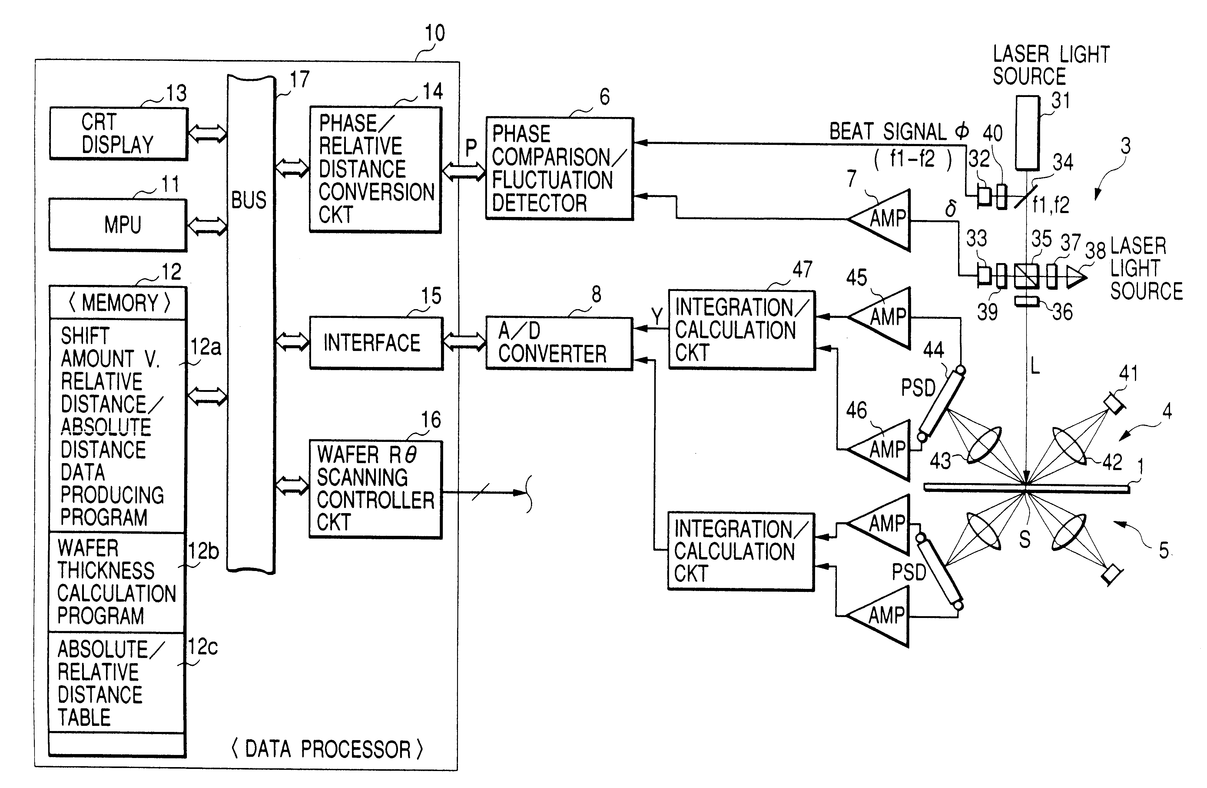
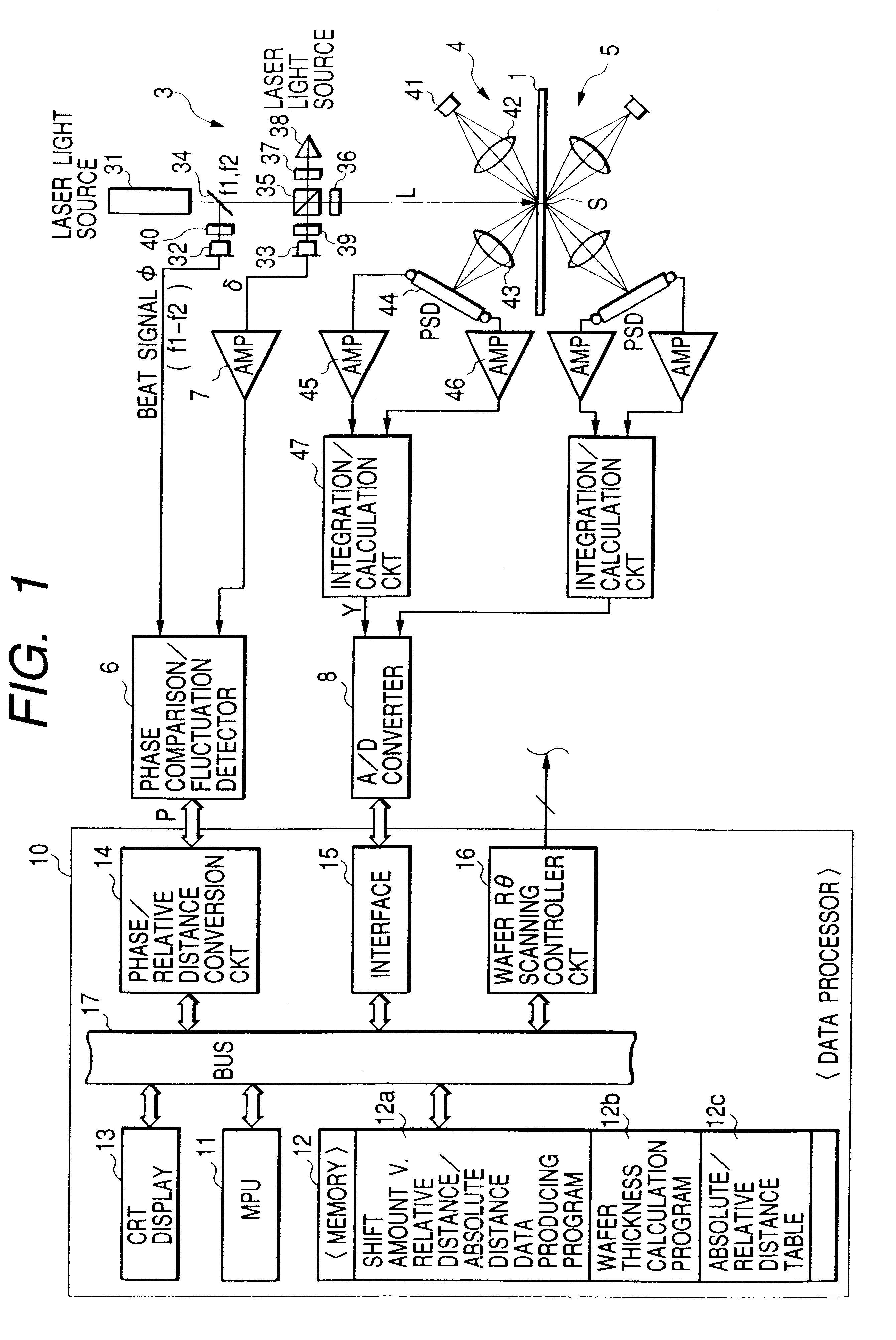
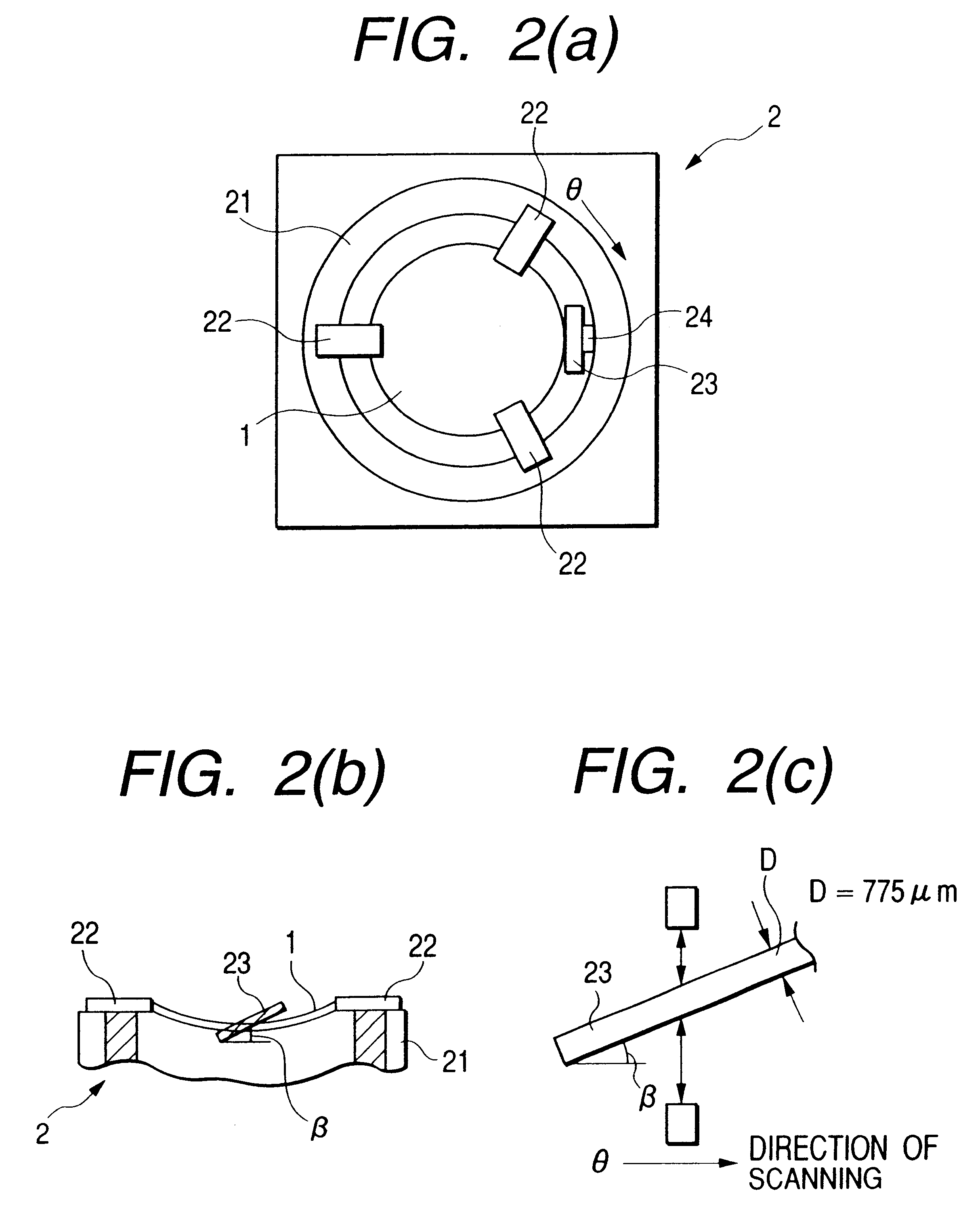
FIG. 1 shows the structure of an embodiment of a wafer thickness measuring apparatus according to the present invention; FIGS. 2(a) to (c) show views for explaining a wafer rotating table; FIG. 3 shows a flow chart of processes therefor; and FIG. 4 is a view for explanation of an absolute / relative distance conversion table therefor.

In the FIG. 1, a wafer 1 (including semiconductor wafers, magnetic head wafers, magnetic discs, etc.) is mounted on a rotating table 2 (see FIGS. 2(a) to (c)), and in an upper portion of the wafer 1 is provided a measurement equipment 3 of optical heterodyne interference for use in the flatness measurement of the wafer, wherein a laser beam L for measuring is irradiated upon it from the optical heterodyne interferometer measurement equipment 3, vertically.

Further, corresponding to the irradiation position (i.e., measurement point) S, ...


PUM


Abstract

In a wafer thickness measuring apparatus and a method thereof, detection values are obtained from a sample piece (for example, a wafer chip) at a plurality of measurement points thereon by first and second detectors for absolute measurement of distances, and at the same time, measurement values of the fluctuations, for relative measurement of distances, are obtained by the optical heterodyne interferometer, and those measurement values are memorized as a plurality of measurement data being related with those measurement values. When measuring the thickness of a wafer, the measurements are performed at measurement points on the wafer which has a front surface and a reverse surface in height lying within the height of the sample piece, on which such a correspondence is obtained, thereby obtaining the detection values of the first and second detectors. Searching conversely from those detection values by referring the correspondence data, the respective detection values are converted into the data of the relative fluctuations therefrom upon the basis of the thickness of the sample piece, thereby obtaining the relative amounts of fluctuation in positions (i.e., the distances) upon the basis of the thickness of the sample piece, respectively. Then, by conducting addition and/or subtraction of the fluctuation amount on the front surface and the reverse surface from the thickness of the sample piece as a reference, it is possible to calculate out the thickness of the wafer to be measured.

Description

1. Field of the InventionThe present invention relates to a wafer thickness measuring apparatus and a method thereof, and in more details, to a wafer thickness measuring apparatus and a method thereof, applying measurement by means of an optical heterodyne interference thereto, for performing the measurement in the distance between relative positions (i.e., a length measurement), being able to perform absolute length measurement exceeding the wave-length of a light thereof, thereby enabling the measurement with an accuracy by means of the optical heterodyne interference.2. Description of Prior ArtAs one of items to be measured when conducting measurement in the flatness of a wafer, a measurement in thickens of the wafer is listed up. In recent years, the thickness of the wafer comes to be thinner gradually, and therefore, at present, there is required a reproducibility of measurement of length being equal or less than .+-.0.5 .mu.m as the accuracy for it.The flatness measurement of ...

Claims


Application Information

Patent Timeline
IPC IPC(8): G01B11/06
CPCG01B11/0691G01B11/06
Inventor ISHIMORI, HIDEONAKAJIMA, HIROSHI
Owner HITACHI ELECTRONICS ENG CO LTD
Why Eureka
Try Eureka