
High-insulated stud and printed circuit board therewith

a technology of printed circuit boards and studs, which is applied in the field of high-insulated studs, can solve the problems of increased cost, increased cost, and difficulty in making universal parts

Inactive Publication Date: 2002-10-08
AGILENT TECH INC
View PDF4 Cites 5 Cited by
  • Summary
  • Abstract
  • Description
  • Claims
  • Application Information

AI Technical Summary

Problems solved by technology

By means of this technology, mounting density is improved somewhat, but a special relay is used and therefore, cost is increased.
Moreover, the heights and spacing of the extensions of the metal conductors used to connect relays is determined from the layout of each part and the board, and therefore, there are problems in that it is difficult to make universal parts and cost is increased.
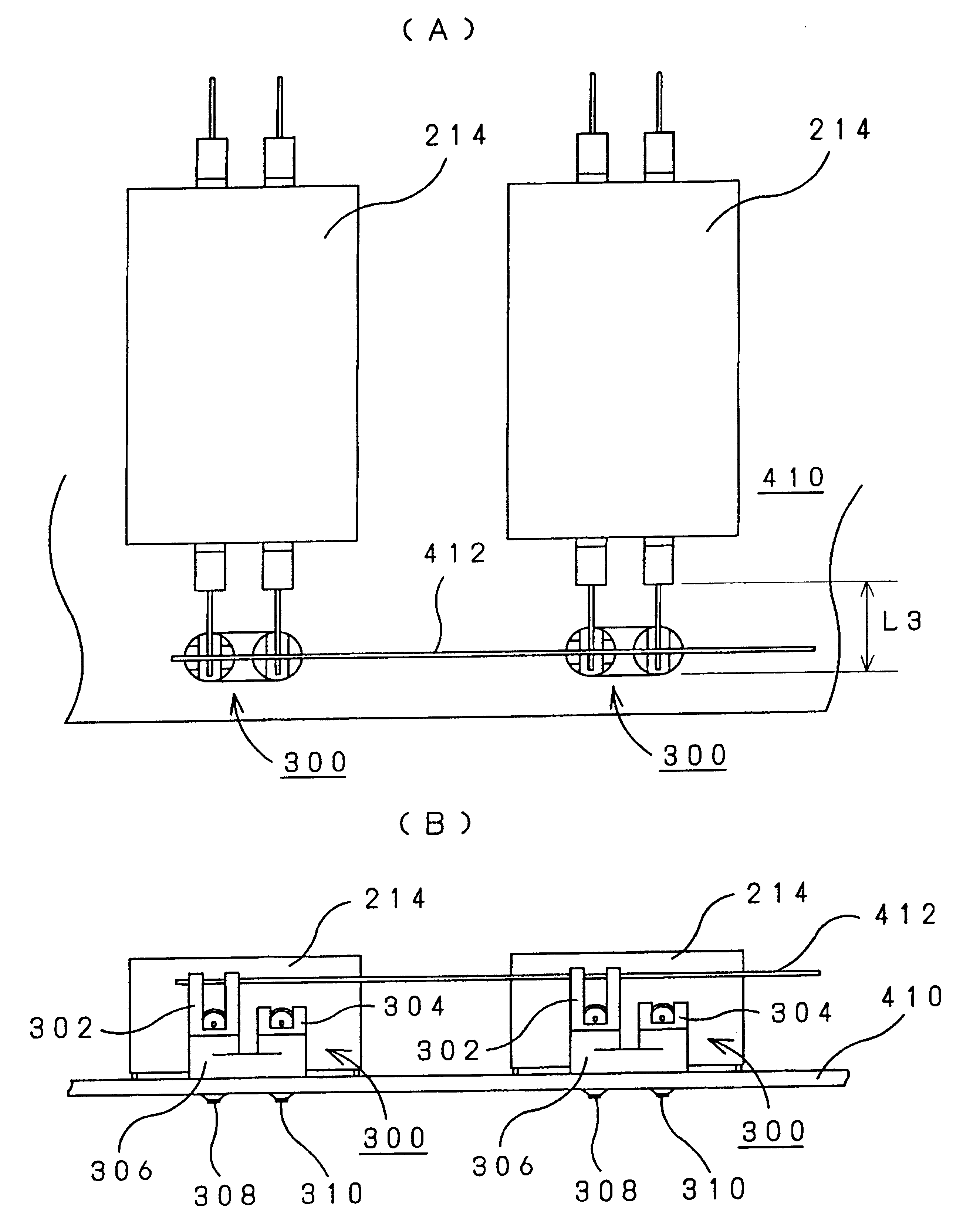
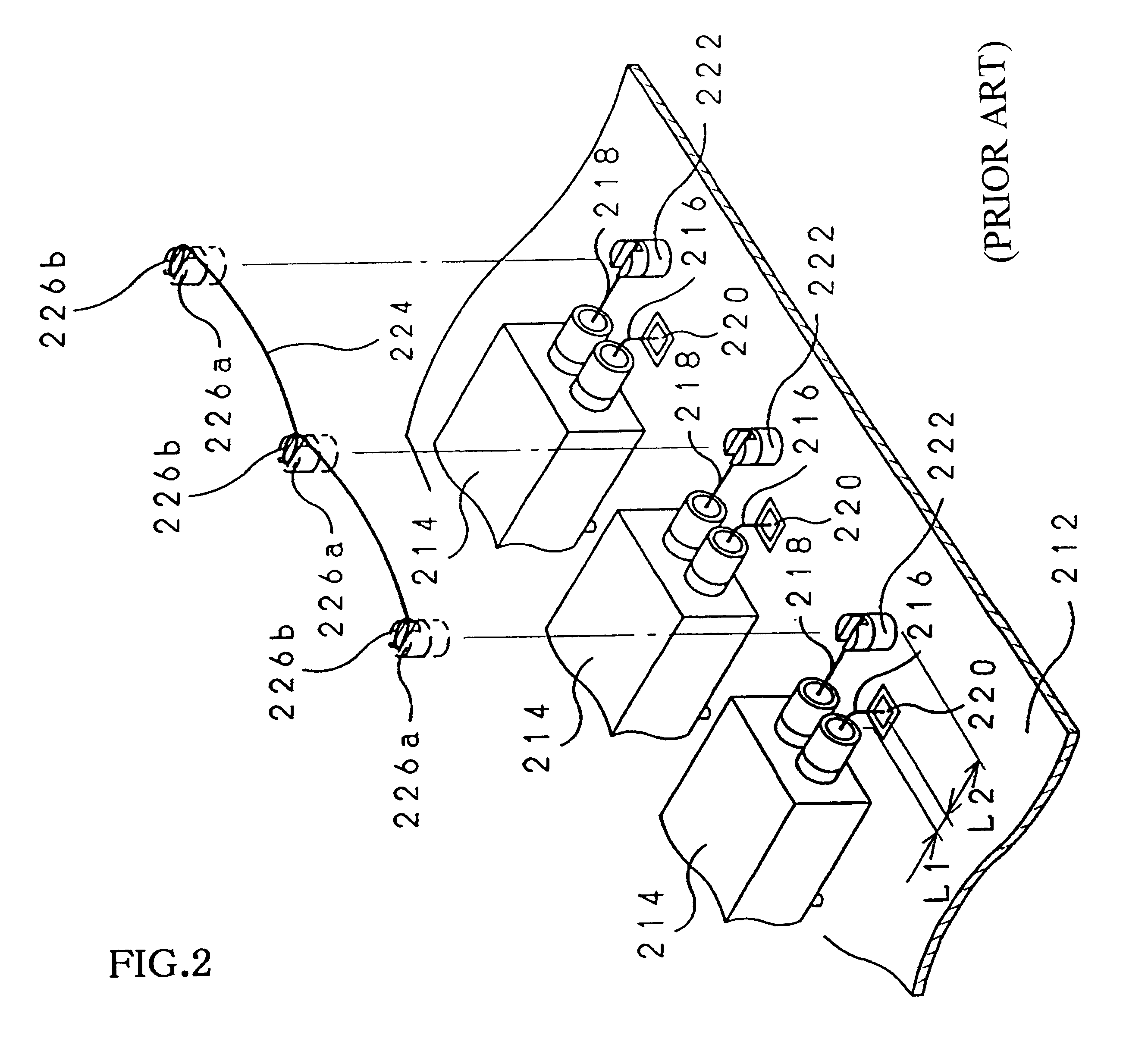
First, the work involving coiling lead 224 around this top part 226b is quite delicate, and therefore, working cost is increased, because a columnar high-insulated stud as small as 3 millimeters in diameter is generally used for efficient use of surface area.
However, the surface area that is occupied will increase and mounting efficiency will drop.
Third, because the work involved in bending guard lead 216 to the position on land 220 is a delicate operation, working cost is increased.
Cracks are made in the glass tube in which the reed switches have been inserted by the tools used to apply pressure and as a result, the percent of defective units increases.

Method used


Image

  • High-insulated stud and printed circuit board therewith
  • High-insulated stud and printed circuit board therewith
  • High-insulated stud and printed circuit board therewith

Examples


first embodiment

High-insulated stud 300 of the present invention is shown in FIG. 3. High-insulated stud 300 has first conductive terminal 302 of a first height, second conductive terminal 304 of a second height lower than the first height, and pins 308 and 310 on platform 306 made from insulation, such as Teflon, etc. There is first groove 312 open at the top and shallow second groove 314 that intersects groove 312 at the top of first conductive terminal 302. Moreover, there is third groove 316 open at the top and having a bottom face of approximately the same height as the bottom face of the first groove at the top of the second conductive terminal. The spacing of the first and second conductive terminals (302, 304) and the first and third grooves (312, 316) on the same platform is designed so that it matches the spacing of the reeds that extend from the reed switches of the reed relay.

First conductive terminal 302 and pin 308 are separate so that they can be understood from the cross section sho...

second embodiment

the high-insulated stud of the present invention is shown in FIG. 6. The high-insulated stud in FIG. 6 is the same as the high-insulated stud in FIG. 3, with the exception that it branches into first stud 602 and second stud 604 and the pedestal branches into first pedestal 606 and second pedestal 608. Consequently, the internal structure and mounting method are also the same and their description is therefore omitted.

By means of this embodiment, there are not 2 or more pins and as a result, there may be problems with matching the leads of the relay and the grooves in the studs. However, this problem can be solved by using a pin with a cross section shape having direction, such as a square, etc.

An oblique view of high-insulated studs 602 and 604 shown in FIG. 6 mounted on a printed board is shown in FIG. 9. It is the same as in FIG. 4 and therefore, a detailed description is omitted.

third embodiment

FIG. 7 is an oblique view of high-insulated stud 700 of the present invention. It is the same as in FIG. 3, with the exception that what corresponds to second groove 314 of FIG. 3 is shown as second groove 706 open sideways near the top of the first conductive terminal. The bottom face of second groove 706 should be higher than the top of the second conductive terminal so that the connecting leads that have been mounted will not be connected to second conductive terminal 304. Incidentally, 704 is the first groove. Consequently, the internal structure and mounting method are the same as shown in FIG. 3 and a description is omitted here.

Furthermore, soldering of the connecting leads to the second groove is performed from the side and not from the top. However, enough clearance for the soldering operation can be guaranteed because the leads project above the other electronic parts.

Moreover, second groove 706 opens only horizontally to the side in this figure. However, various modificat...


PUM

PropertyMeasurementUnit
diameteraaaaaaaaaa
distanceaaaaaaaaaa
distanceaaaaaaaaaa

Abstract

A high-insulated stud comprises a first columnar conductive terminal of a first height, a second columnar conductive terminal of a second height lower than the height of the first conductive terminal that is placed in a row with and at a distance from the first conductive terminal, an insulating pedestal, and a first groove open at the top and a second groove intersecting the first groove and shallower than the first groove at the top of the first conductive terminal and a third groove open at the top, which is parallel with the first groove and whose bottom face is almost the same height as the bottom face of the first groove, at the top of the second conductive terminal.

Description

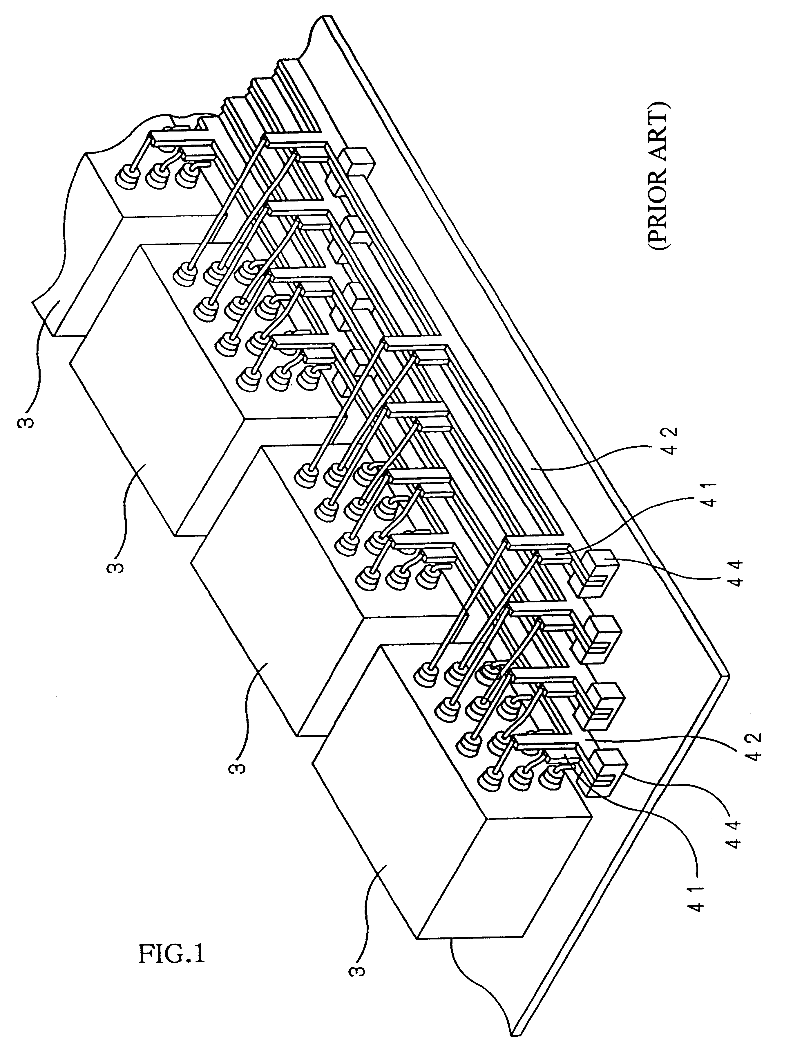
1. Field of the InventionThe present invention relates to a high-insulated stud and in further detail, to a high-insulated stud that connects multiple reed relays and a printed circuit board (printed board) that uses this high-insulated stud.2. Description of the Prior ArtThe technology disclosed in Utility Model Laid-Open No. Sho 63(1988)-73,836 shown in FIG. 1 is known as a conventional high-density, high-insulation mounting method by means of which multiple relays housing multiple reed switches are connected.An example is shown in FIG. 1 where reed relay 3 houses reed switches in 3 vertical rows and 4 horizontal rows and the reeds at positions corresponding to adjacent relays themselves are connected. The highest reeds bend away slightly to the left and the second-highest reeds bend away slightly to the right. Metal conductors 41 and 42 with an extension at appropriate heights and spacing for each reed of the multiple relays are soldered to the reeds.Metal conductors 41 and 42 ar...

Claims


Application Information

Patent Timeline
Patent Type & Authority Patents(United States)
IPC IPC(8): H01H51/00H01H51/28H05K3/30H01B17/00H01H45/14H05K1/16H05K1/18
CPCH01H51/281H05K3/301H01R12/718
Inventor UCHIDA, MINORUSHIMIZU, HIROYUKICHIKAMATSU, KIYOSHI
Owner AGILENT TECH INC
Learn More