
Method of burning in an integrated circuit chip package

a technology of integrated circuits and chips, applied in the direction of electronic circuit testing, measurement devices, instruments, etc., can solve the problems of high power levels during burn, long burnin procedure, and relatively high voltage and temperatur

Inactive Publication Date: 2003-06-10
GOOGLE LLC
View PDF17 Cites 17 Cited by
  • Summary
  • Abstract
  • Description
  • Claims
  • Application Information

AI Technical Summary

Problems solved by technology

The burn-in procedure usually takes many hours and includes subjecting each of the chips or chip packages to relatively high voltages and temperatures.
The high voltage results in high power levels during burn-in.
For example, it is common for the test parameters of the chip to be set at 120A.degree. C. plus or minus 5A.degree. C. If during testing the temperature of the chip exceeds the maximum allowable temperature, i.e. about 125A.degree. C. in this case, a relatively high likelihood of damage to the chip is the result, thus damaging a chip that would otherwise be a good and serviceable chip if tested within the temperature parameters set by the te
ion. However, even when these are present, and they actuate, this burn-in station is rendered non-functioning, and thus the chip at this station is not burne
d-in. This results in a lower equipment effic
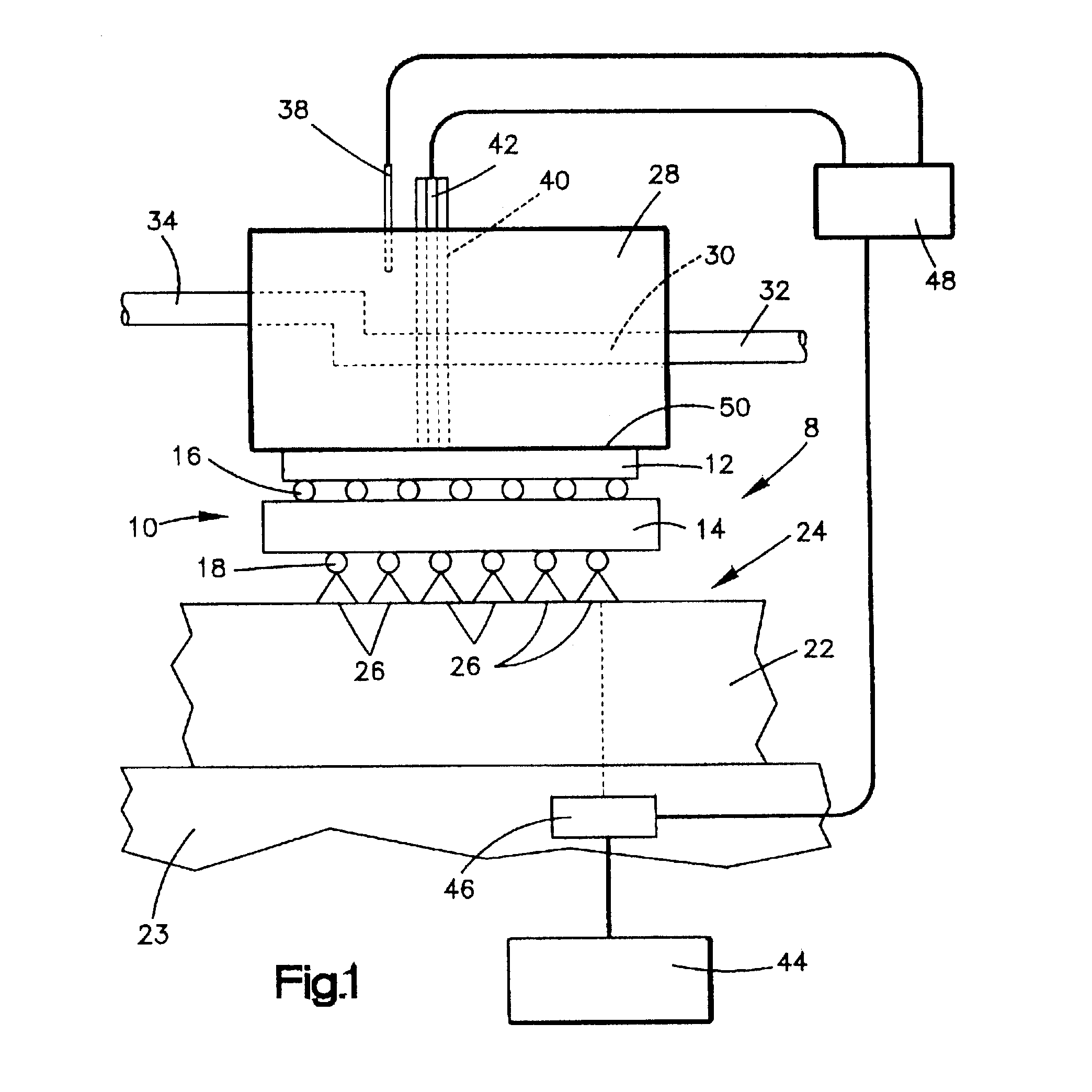
For example, differences in surface finish or flatness of the various heatsinks for each individual chip package can cause significant variation in thermal resistance; also, different surface finish or flatness of the back side of the chip which is in contact with the heatsink can also cause differences in the thermal resistance.
Too high a thermal resistance at the interface between the heatsink and the chip can result in thermal heating of the chip above allowable limits, thus destroying what might otherwise be a perfectly good chip.

Method used


Image

  • Method of burning in an integrated circuit chip package
  • Method of burning in an integrated circuit chip package
  • Method of burning in an integrated circuit chip package

Examples


Embodiment Construction

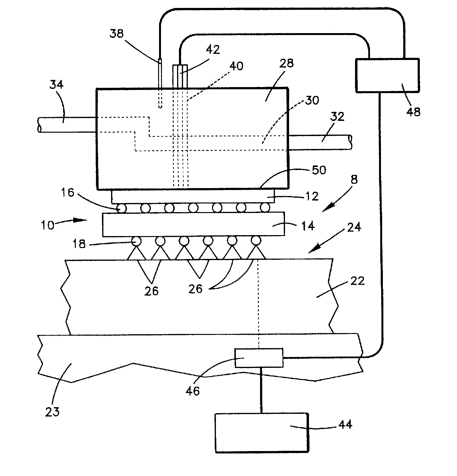
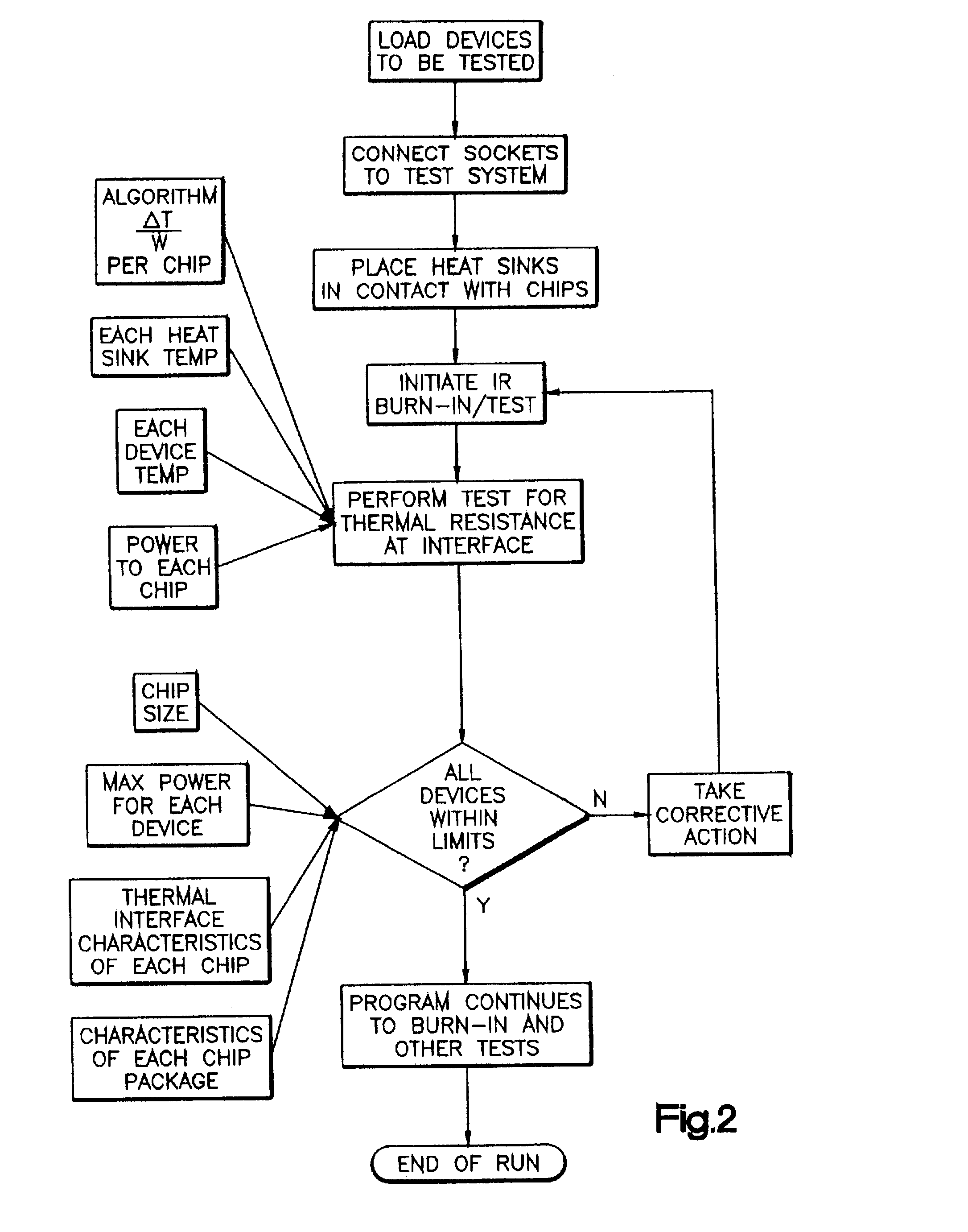
--measured chip temperature -87A.degree. C. heatsink temperature measured -27A.degree. C. measured power to this chip a{character pullout}" 80 watts Thus, thermal resistance at the interface can be calculated as follows: 87A.degree. C. minus 27A.degree. C. (I"T) divided by 80 watts (w) equals 60A.degree. C. divided by 80 watts equals 0.75A.degree. C. per watt (TR). ##EQU2##

This is greater than the calculated maximum allowable thermal resistance of 0.67 watts per degree centigrade and, thus, this chip should not be subjected to the burn-in procedure at 150 watts and 120A.degree. C. plus or minus 5A.degree. C. Example 2--measured chip temperature -67A.degree. C. heat sink temperature -27A.degree. C. power measured to this chip -72 watts The thermal resistance is then calculated as follows: 67A.degree. C. minus 27A.degree. C. (I"T) divided by 72 watts (w) equals 40A.degree. C. divided by 72 watts equals 0.55A.degree. C. per watt (TR) ##EQU3##

Since this value is less than the calculated...


PUM


Abstract

An improved method of burn-in of I / C chips is provided wherein, at the beginning of the burn-in process, the thermal resistance between the heatsink and the chip is measured at reduced power, the maximum allowable thermal resistance between the chip and heatsink interface is calculated and compared to the actual thermal resistance of the interface. If the actual thermal resistance measured at the interface between the heatsink and the chip package is greater than the maximum allowable calculated thermal resistance, then the corrective action is initiated in order to prevent damage to the I / C chip during burn-in or increase efficient use of the test sites.

Description

1. Field of the InventionThis invention relates generally to burn-in procedures for integrated circuit chip packages and, more particularly, to a method for controlling burn-in of integrated circuit chips to prevent damage to the chip by excessive heat build-up resulting from applied power during the burn-in procedure.2. Background InformationIn the manufacture of integrated circuit chips and integrated circuit chip devices or packages, one of the final procedures performed on the chip or chip package is final burn-in and testing. It is important to note that powers seen during burn-in are rapidly increasing over time. Increase in device power over time is attributed to increased static leakage current per device corresponding to CMOS technology advancement. This is a trend that follows technology. The burn-in and testing is generally done on a plurality of chips in chip packages mounted in a fixture. The burn-in procedure usually takes many hours and includes subjecting each of the...

Claims


Application Information

Patent Timeline
Patent Type & Authority Patents(United States)
IPC IPC(8): G01R31/28
CPCG01R31/2874G01R31/287G01R31/2863
Inventor GAMACHE, ROGER G.GARDELL, DAVID L.KNOX, MARC D.
Owner GOOGLE LLC
Learn More