Cassette table of a semiconductor fabricating apparatus

a fabricating apparatus and cassette technology, applied in the field of cassette tables, can solve the problems of collision between a blade and the transfer device of the wafer and the wafer, damage to the wiring pattern or metal line of the wafer, and the damage of the arcing

Inactive Publication Date: 2004-01-20
SAMSUNG ELECTRONICS CO LTD
View PDF4 Cites 230 Cited by
  • Summary
  • Abstract
  • Description
  • Claims
  • Application Information

AI Technical Summary

Problems solved by technology

The arcing can damage wiring patterns or metal lines of the wafer.
In particular, the larger the wafer is, the greater the static electricity affects the wafer in these ways.
Such deviation could result in a collision between a blade and of the wafer transfer device and a wafer when the wafer transfer device picks the wafer from the cassette 20.
This unfavorable phenomenon is more pronounced in wafers having large diameters.
When a wafer charged with the static electricity is handled, arcs are created and the arcs damage portions (a) of the metal lines of the wafer.
Thus, arcing as the result of static electricity accumulated on a wafer lowers the manufacturing yield.
Still further, the static electricity accumulated on the cassette generates electrical interference in the semiconductor fabricating system.
The electric interference causes the semiconductor fabricating system to malfunction.

Method used


Image

  • Cassette table of a semiconductor fabricating apparatus
  • Cassette table of a semiconductor fabricating apparatus
  • Cassette table of a semiconductor fabricating apparatus

Examples


Embodiment Construction

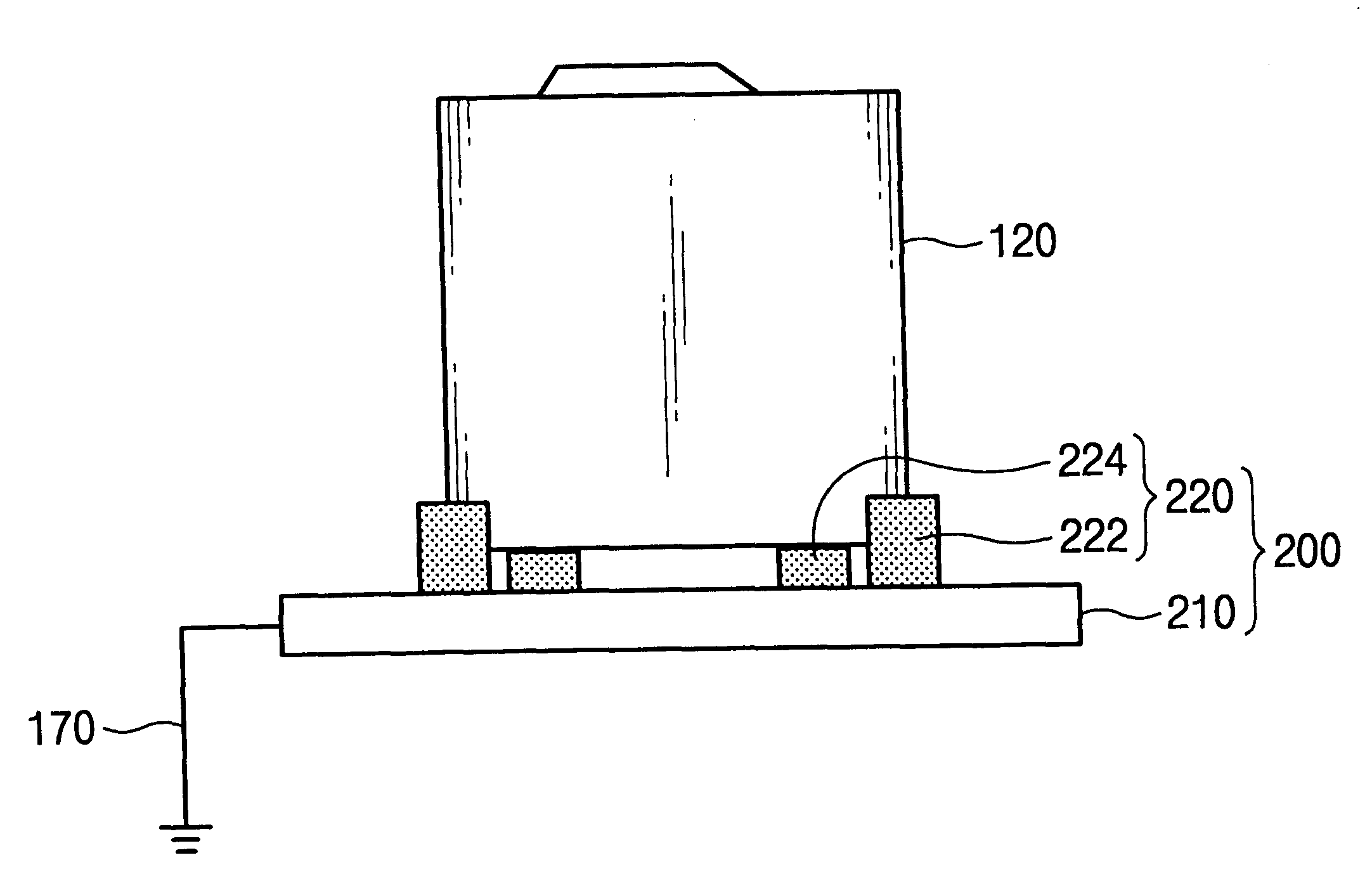
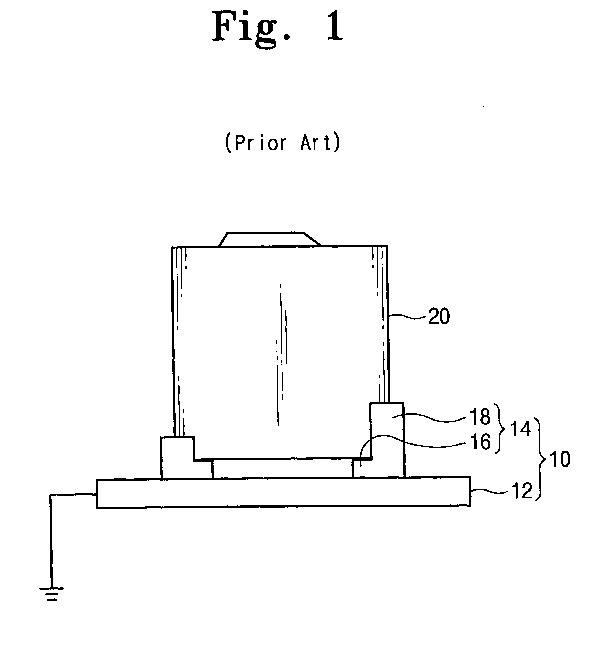
Referring to FIG. 4, a spinner 100 includes a cassette table 200, a first transfer device 130, support pins 140, a second transfer device 150, and processing chambers 160 in which turntables for facilitating a spin-coating operation are provided.

A cassette 120 for receiving wafers is located on the cassette table 200. Wafers are transferred from the cassette 120 to the support pins 140 by the first transfer device 130. From there, wafers are processed in the processing chambers 160. More specifically, the wafers are spun rapidly in the processing chambers 160 in order to carry out a coating process. The fast-rotating wafers are thus charged with static electricity. Subsequently, these wafers are returned to the cassette 120 by the second transfer device 150. The first transfer device 130 re-loads the returned wafers into the cassette 120.

Wafer-contacting parts of the first transfer device 130, the second transfer device 150, and the support pins 140 are made of urethane or non-condu...


PUM


Abstract

A cassette table on which a wafer cassette is supported allows static electricity to be discharged from the cassette and hence, form the wafers disposed in the cassette. The cassette table includes a top plate, a cassette supporter that is mounted on the top plate and supports the cassette. At least part of the cassette supporter is made of a material that allows static electricity to be discharged to ground therethrough.

Description

1. Field of the InventionThe present invention relates to a semiconductor fabricating apparatus. More particularly, the present invention relates to a cassette table for supporting a wafer cassette outside a processing chamber.2. Description of the Related ArtIn a semiconductor fabricating system, a spinner or a scrubber rapidly rotates a wafer that is being processed. Static electricity occurs on the fast-rotating wafer due to friction between the wafer and air or de-ionized water (DI water). When the wafer is charged with static electricity, large numbers of particles will electro-statically adhere to the wafer. Also, arcing occurs during wafer handling. The arcing can damage wiring patterns or metal lines of the wafer. In particular, the larger the wafer is, the greater the static electricity affects the wafer in these ways.These problems are exacerbated by a conventional cassette table having non-conductive cassette supporters, as shown in FIG. 1. After a spinner or a scrubber r...

Claims


Application Information

Patent Timeline
Patent Type & Authority Patents(United States)
IPC IPC(8): H01L21/67H01L21/673H01L21/02B65D85/86H01L21/677H01L21/68
CPCH01L21/67396Y10S414/137Y10S414/14H01L21/67775H01L21/68
Inventor HAM, DONG-SEOKLEE, KUN-HYUNGKIM, HYEOGI-KIPARK, KYOUNG-HO
Owner SAMSUNG ELECTRONICS CO LTD
Why Eureka
Try Eureka