Graphics engine command FIFO for programming multiple registers using a mapping index with register offsets

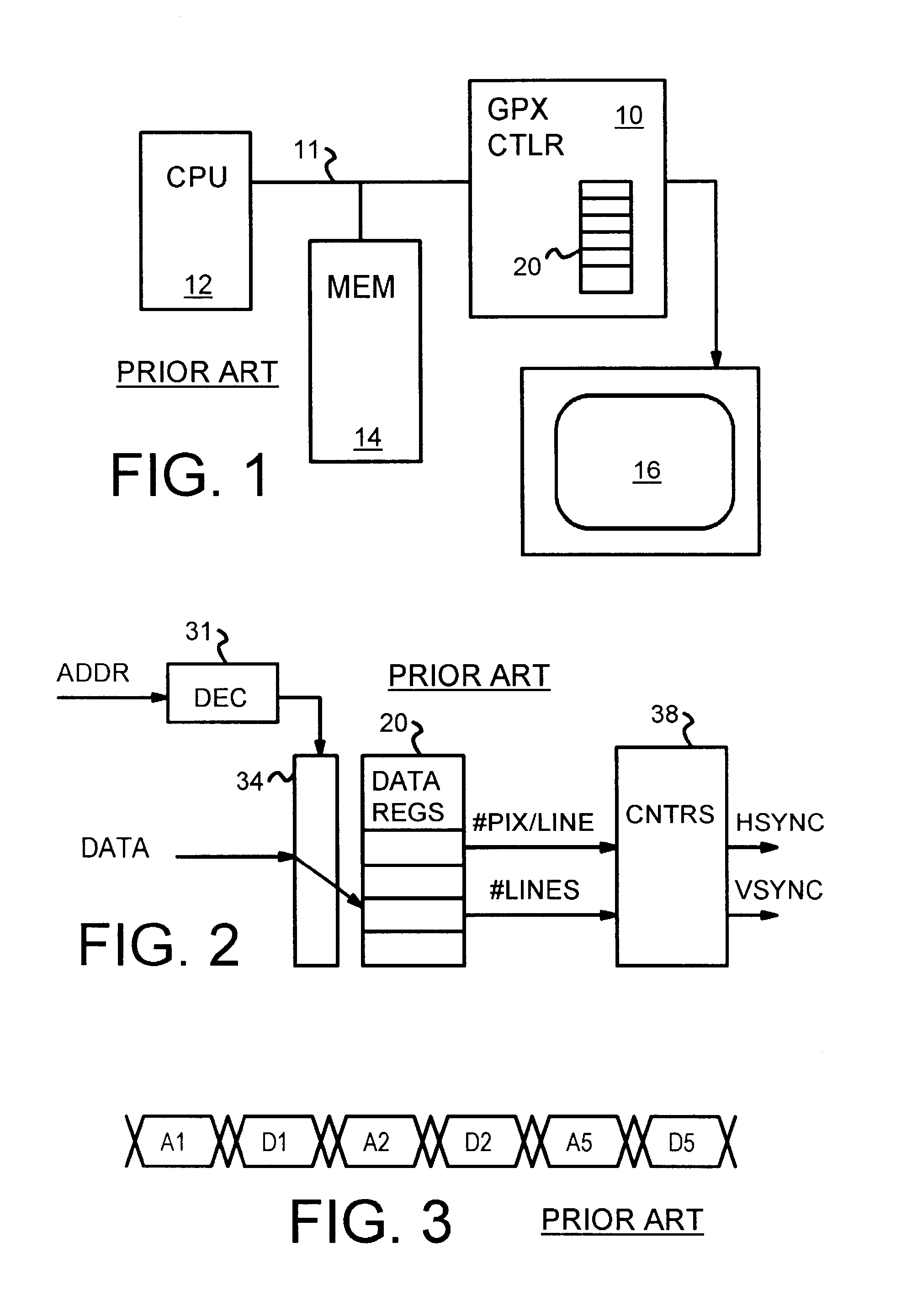
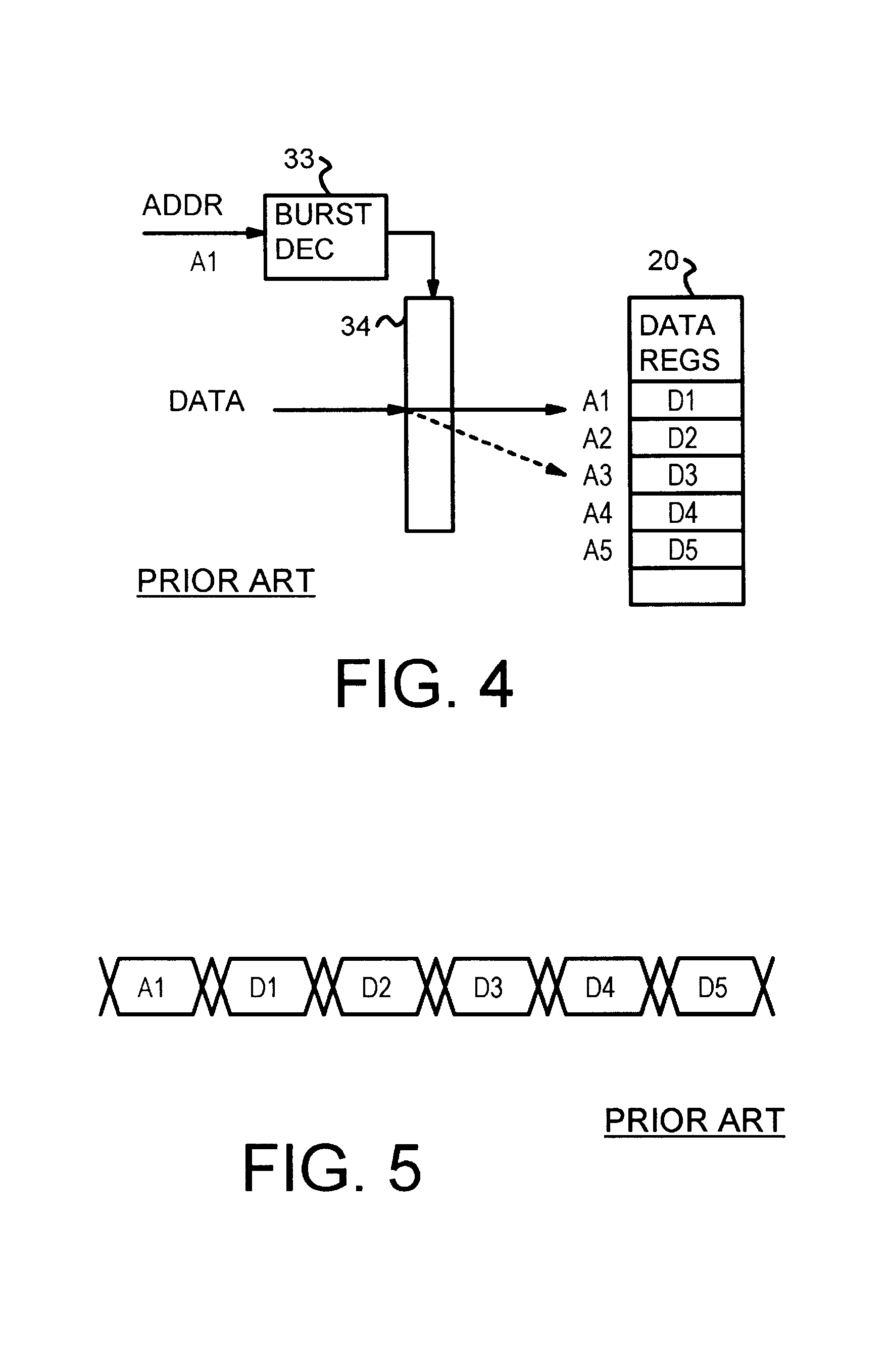
a mapping index and register offset technology, applied in the field ofgraphics systems, can solve the problems of inability to write registers, inability to burst access, and limited number of i/o addresses available to peripheral controller chips

Inactive Publication Date: 2004-05-25
SERVSTOR TECHNOLOGIES LLC +1
View PDF16 Cites 11 Cited by
  • Summary
  • Abstract
  • Description
  • Claims
  • Application Information

AI Technical Summary

Problems solved by technology

Thus the number of I/O addresses available to a peripheral controller chips is often limited.
Since registers A3, A5 are not being written, a burst

Method used


Image

  • Graphics engine command FIFO for programming multiple registers using a mapping index with register offsets
  • Graphics engine command FIFO for programming multiple registers using a mapping index with register offsets
  • Graphics engine command FIFO for programming multiple registers using a mapping index with register offsets

Examples


Embodiment Construction

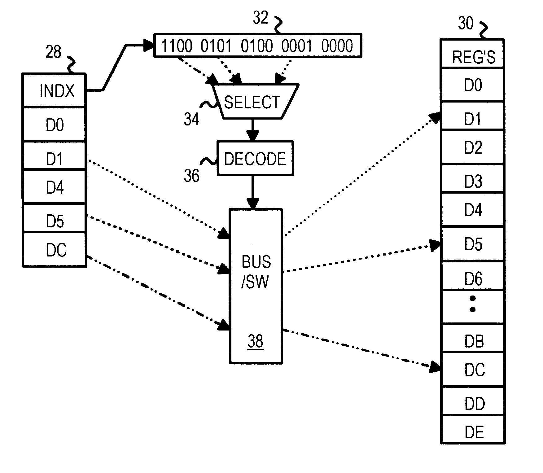
Several other embodiments are contemplated by the inventor. For example, several different mapping index words may be used, each with a different starting address or different command FIFOs for a different bank of registers. The second mapping index word may refer to the next set of registers that are offset by an additional 15 registers or some other offset. When all mapping indexes in the first index are 0xF, then no registers in the first bank are programmed. Alternately, another bank field may be added to the index to indicate which bank is to be programmed. This bank field can be decoded to select one bank from among several banks. The bank field could be located in a programmable register rather than in the index, or some other means such as an I / O pin could be used to select banks. Byte, word, double-word, or other addressing may be used. Additional restrictions may be placed on the mapping index word, such as requiring that the disabled mapping fields be the MSB's or that at...


PUM


Abstract

A host writes graphics commands and data to programmable registers through a command FIFO that is read by a graphics controller or BitBlt engine. Rather than write an address and a data value for each register programmed, the host writes one address, one index, and several data values. The address points to an index register. The index is a mapping index word with several multi-bit mapping fields. Each multi-bit mapping field in the index identifies a register to be programmed with one of the data values. Since N bits are used for each mapping field, the mapping field can select one register in a bank of 2<N>-1 registers. The registers in the bank can be programmed in any order, and registers can be skipped. Since only one index is stored in the command FIFO for programming several registers, less memory space and fewer bus cycles are required.

Description

BACKGROUND OF INVENTIONThis invention relates to graphics systems, and more particularly to addressing of programmable registers.Personal computers (PCs) and other computer systems have a variety of controller integrated circuits (ICs) or chips that control subsystems such as for graphics, disks, and general system logic. Such controller chips are usually programmable. For example, the graphics controller can be programmed with the display resolution, such as the number of pixels in a horizontal line, or the number of lines on a screen. Memory-controller chips can be programmed with numbers of clock cycles for memory accesses, so that the timing signals generated by the controller chip can be adjusted for faster memory chips or faster bus clocks.Advanced graphics systems often employ specialized engines, such as a bit-block-transfer BitBlt engine. Graphics data and commands can be written to a command first-in-first-out (FIFO) by a host processor, allowing the BitBlt engine to read ...

Claims


Application Information

Patent Timeline
IPC IPC(8): G09G5/36G06F3/14G06F9/30G06F9/355G06F9/38
CPCG06F3/14G06F9/30043G06F9/30101G06F9/345G06F9/355G06F9/3879G09G5/363
Inventor RETIKA, JOHN Y.
Owner SERVSTOR TECHNOLOGIES LLC
Why Eureka
Try Eureka