Semiconductor package

a technology of semiconductors and packaging, applied in the direction of stools, seating furniture, electric devices, etc., can solve the problems of increasing heat dissipation, and achieve the effects of less mounting height and footprint, improved thermal performance, and increased functionality and reliability

Inactive Publication Date: 2005-02-22
AMKOR TECH SINGAPORE HLDG PTE LTD
View PDF88 Cites 128 Cited by
  • Summary
  • Abstract
  • Description
  • Claims
  • Application Information

AI Technical Summary

Benefits of technology

The present invention provides semiconductor packages that can be made smaller than the conventional packages described above, so as to have a lesser mounting height and footprint, while providing increased functionality and reliability and improved thermal performance.

Problems solved by technology

In addition, a surface of the semiconductor chip may be exposed through the package body, further increasing heat dissipation.

Method used


Image

  • Semiconductor package
  • Semiconductor package
  • Semiconductor package

Examples


first embodiment

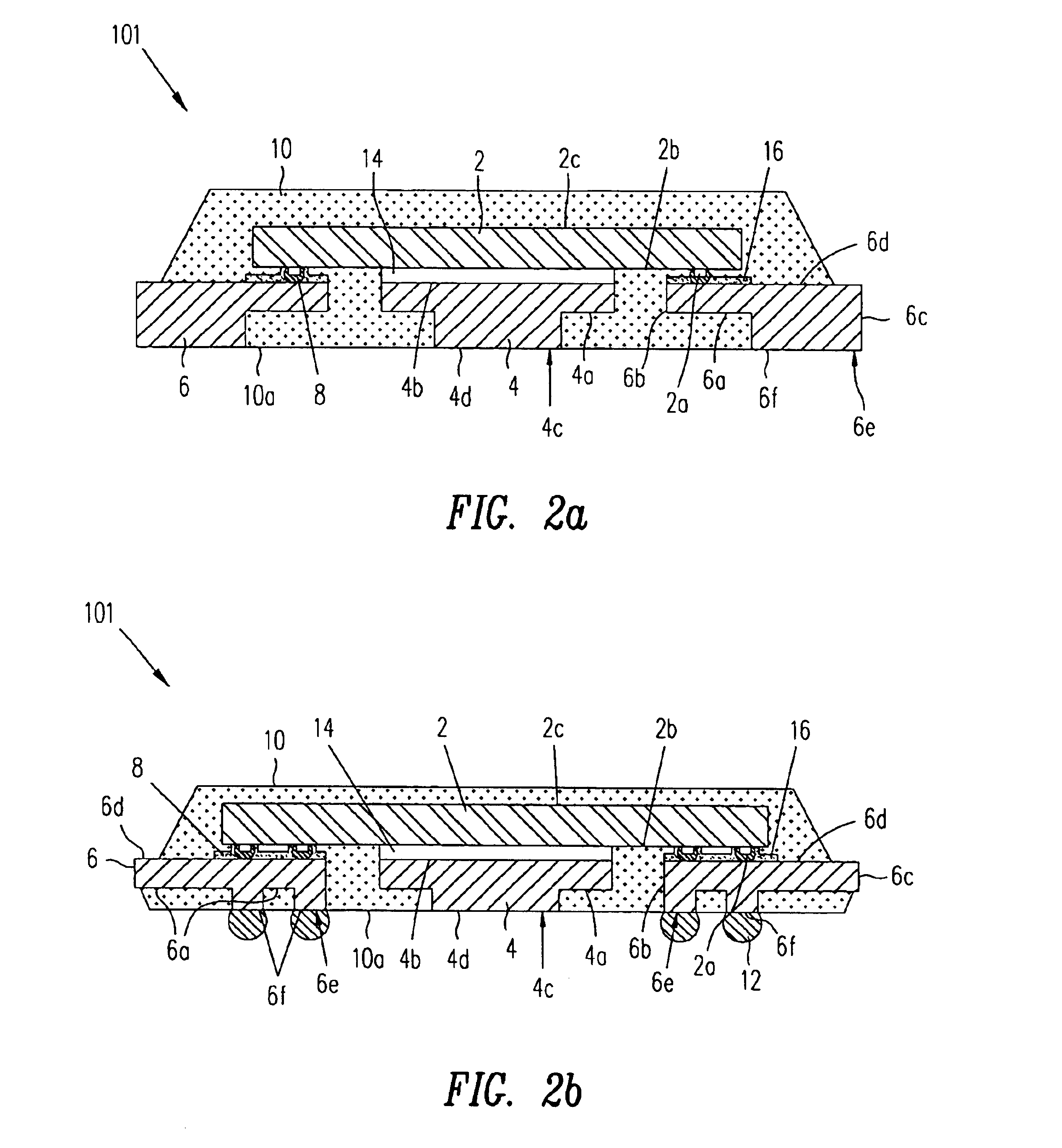
FIGS. 2a and 2b show a semiconductor package 101 according to the present invention. Semiconductor package 101 includes many of the same features as package 100 of FIG. 1. Hence, our discussion focuses on differences between this embodiment (and those that follow) and the conventional package of FIG. 1.

Semiconductor package 101 includes a semiconductor chip 2, which has a plurality of peripheral input-output pads 2a along edges of active surface 2b. First side 4b of chip mounting substrate 4 is attached by an adhesive 14 to an open central portion of active surface 2b of chip 2 fully inside of peripheral input / output pads 2a. A plurality of leads 6 are placed about the peripheral line of chip mounting substrate 4, each spaced a selected lateral distance from the chip mounting substrate 4. In an alternative embodiment, chip mounting substrate 4 is omitted.

Chip mounting substrate 4 of FIG. 2a includes a recessed horizontal surface 4a that fully surrounds central surface 4d of bottom s...

second embodiment

FIG. 3a and FIG. 3b show a semiconductor package 102 according the present invention, which differs only slightly from semiconductor package 101 of FIGS. 2a and 2b. Accordingly, our discussion will focus on the differences between the packages.

In FIGS. 3a and 3b, semiconductor chip 2 includes a plurality of peripheral bond pads 2a along the edges of active surface 2b, and in addition includes at least one or a plurality of central bond pads 2a at a central portion of active surface 2a inward of the peripheral bond pads 2a. The central input-output pads 2a of chip 2 each face a portion of upper first side 4b of chip mounting substrate 4, and may be used for ground / power inputs to chip 2. The central input-output pads 2a are each electrically connected in a flip-chip style to the upper first side 4b of chip mounting substrate 4 by a conductive connecting means 8. First side 4b of chip mounting substrate 4 may be coated with an insulating layer 16 through which the conductive connectin...
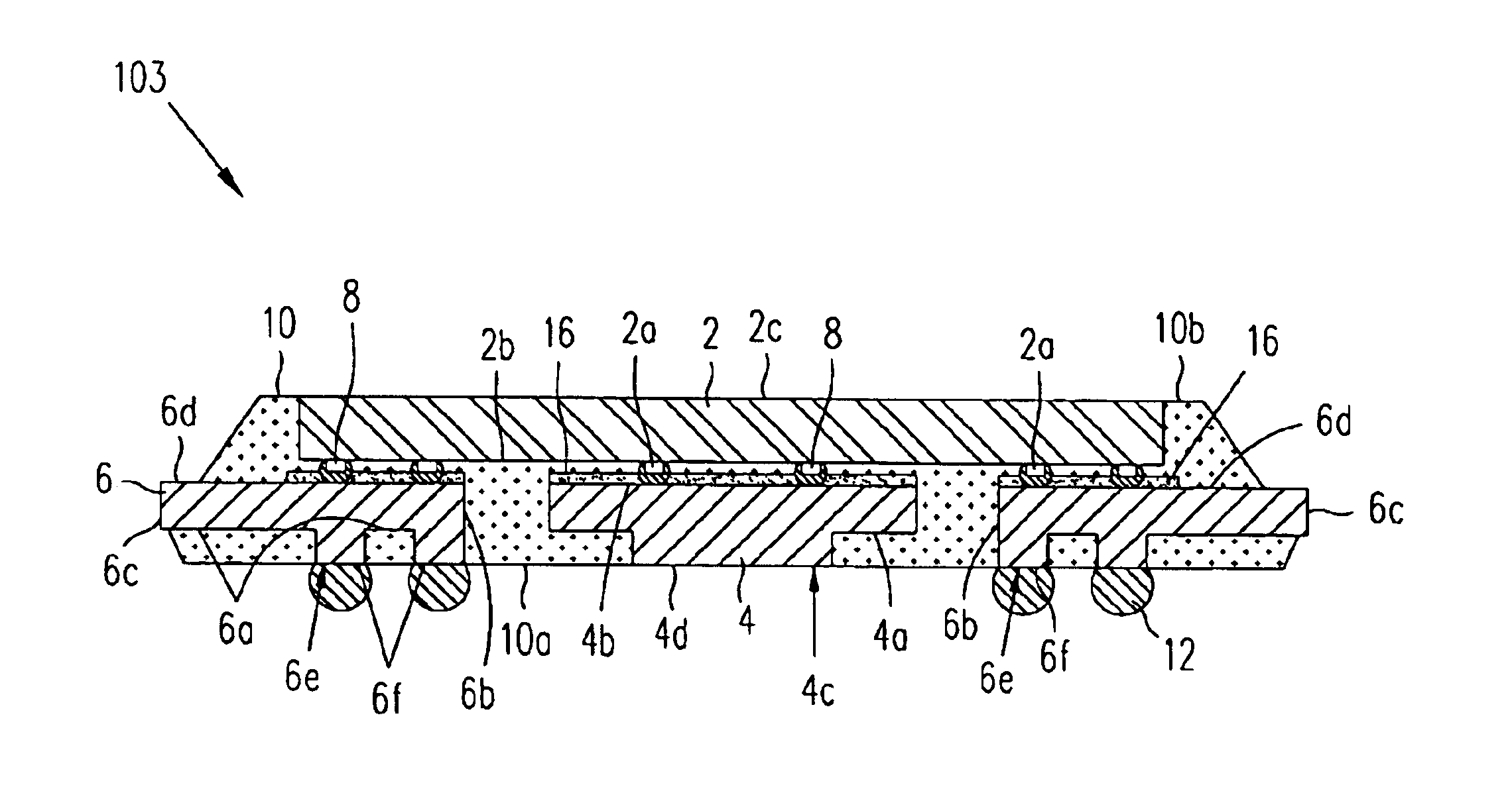
third embodiment

FIGS. 4a and 4b show a semiconductor package 103 according to the present invention. Package 103 of FIGS. 4a and 4b is the same as package 102 of FIGS. 3a and 3b, except that inactive surface 2c of semiconductor chip 2 is exposed to the outside in the horizontal plane of upper exterior surface 10b of package body 10. Thus, heat generated in semiconductor chip 2 can be rapidly emitted to the outside through exposed inactive surface 2c, thereby enhancing the thermal performance of the package.

FIG. 5 is a plan view of a central portion of a leadframe 18 that may be used to make exemplary semiconductor packages 101, 102, and 103, typically where conductive connection means 8 is a metal ball. Leadframe 18 includes a chip mounting substrate 4, on which semiconductor chip 2 is to be mounted, and tie bars 20 that extend diagonally from respective corners of chip mounting substrate 4. Leads 6 are radially formed about the peripheral line of the chip mounting substrate 4. Practitioners will a...


PUM


Abstract

A semiconductor package is disclosed that bonds a semiconductor chip to a leadframe using a flip chip technology. An exemplary semiconductor package includes a semiconductor chip having a plurality of input-output pads at an active surface thereof. A plurality of leads are superimposed by the bond pads and active surface of the semiconductor chip. The leads have at least one exposed surface at a bottom surface of the package body. A plurality of conductive connecting means electrically connect the input-output pads of the chip to the leads. A package body is formed over the semiconductor chip and the conductive connecting means. The bottom surface portions of the leads are exposed to the outside.

Description

BACKGROUND OF THE INVENTION1. Field of the InventionThe present invention is in the field of semiconductor packaging.2. Description of the Related ArtThere are trends in semiconductor packaging towards packages that are highly functional, yet increasingly smaller in size so as to provide higher density in mounting. In keeping with these trends, semiconductor package 100 of FIG. 1 includes a semiconductor chip 2 which has a plurality of input-output pads 2a on a top, active surface 2b thereof. An opposite bottom, inactive surface 2c of chip 2 is bonded to a metal chip mounting substrate 4 by an adhesive 14.Chip mounting substrate 4 has a top first side 4b bonded to chip 2 by adhesive 14, and an opposite second side 4c. Second side 4c includes an exposed bottom central surface 4d. Second side 4c of chip mounting substrate 4 has been partially etched around central surface 4d so as to form a recessed horizontal surface 4a that fully surrounds and is vertically recessed from central sur...

Claims


Application Information

Patent Timeline
Patent Type & Authority Patents(United States)
IPC IPC(8): H01L23/495H01L21/02H01L21/60H01L23/48
CPCH01L23/4951H01L24/83H01L23/49548H01L24/29H01L24/32H01L2924/014H01L2224/16245H01L2224/32245H01L2224/48091H01L2224/48247H01L2224/48465H01L2224/73203H01L2224/73265H01L2224/8319H01L2224/838H01L2924/01046H01L2924/01047H01L2924/01079H01L2924/01082H01L2924/0781H01L2924/15311H01L2224/29101H01L24/48H01L2924/01033H01L2924/00014H01L2924/00H01L2924/00012H01L24/73H01L2224/05599H01L2224/85399H01L2924/181H01L2224/45015H01L2924/207H01L2224/45099A47C7/546
Inventor SEO, SEONG MINCHUNG, YOUNG SUKPAEK, JONG SIKKU, JAE HUNYEE, JAE HAK
Owner AMKOR TECH SINGAPORE HLDG PTE LTD
Why Eureka
Try Eureka