Magnetoresistive sensor including magnetic domain control layers having high electric resistivity

a magnetic domain control and magnetoresistive sensor technology, applied in nanoinformatics, instruments, record information storage, etc., can solve the problems of high loss of s/n of read sensor, difficult to ensure the insulating properties of the magnetic domain control layer, and difficult to provide a sufficient recording magnetic field for read elements, etc., to improve the reproducing resolution of the magnetoresistive sensor. , the effect of high electric resistivity

Inactive Publication Date: 2005-03-22
HITACHI GLOBAL STORAGE TECH JAPAN LTD
View PDF10 Cites 15 Cited by
  • Summary
  • Abstract
  • Description
  • Claims
  • Application Information

AI Technical Summary

Benefits of technology

An object of the present invention is to provide a magnetoresistive sensor having, in particular, excellent reproducing resolution, in magnetic read and write, a magnetic head using the same, and a magnetic disk apparatus, and, for that, to provide magnetic domain control layers having high electric resistivity suitable for improving the reproducing resolution of the magnetoresistive sensor.
Conventionally, the magnetic domain control layer is arranged on the lower magnetic shield by employing a multi-layered structure of insulating layer / (metal underlayer) / hard magnetic metal material layer / insulating layer. In the present invention, there is used means wherein the magnetic domain control layer comprises a single layer made of a hard magnetic material having high electric resistivity, thereby directly performing magnetic domain control. According to this method, the insulating layers arranged at the upper and lower sides of the magnetic layer can be omitted. Thus, when the magnetoresistive sensor layer is made thinner, a loss of the susceptibility due to the thickness of the insulating layer can be reduced, so as to lower the shunting loss of an electric current. In addition, since the magnetic domain control layer is in direct contact with the magnetoresistive sensor layer, the loss of the magnetic field of the magnetic domain control can be minimized.
Examples of the underlayer material for use in this method include CoO (200), MgO (200), NiO (200), EuO (200), FeO (200) and ZnO (001). These materials can be relatively easily grown at room temperature by means of the sputtering method. When a spinel type compound γ-Fe2O3 is grown on this plane, it is found that the γ-Fe2O3 (400) plane can be manufactured on these oxides in a relatively low temperature range below 300° C. These thin oxide films can exhibit a function as the underlayer even in the thickness range of 1 nm to 5 nm. These underlayers are electrically an insulator to insulating semiconductor. Basically, they can eliminate shunting from the magnetoresistive sensor layer to the magnetic domain control layer.

Problems solved by technology

The read sensor has a high loss of S / N when Barkhausen noise is caused, and it is necessary to control this.
Thus, the thickness dependence as the characteristic of the insulating layer or the presence of pinhole cannot maintain the insulating properties, so that an electric current for sensing a signal (sensing current) is leaked to the magnetic shield to reduce read output.
The read element is difficult to provide a sufficient recording magnetic field in a conventional in-plane magnetic recording system.
However, employing such a structure, when the area of the magnetoresistive sensor layer is reduced, there arises a new problem that the conventional magnetic domain control layer is difficult to ensure the insulating properties of the magnetic domain control layer.
The magnetoresistive sensor layer is made thinner and finer; there are imposed three problems: (1) the throwing power of the lower insulating layer is insufficient so as to shunt the sensing current flowing to the magnetoresistive sensor layer to the magnetic domain control layer, resulting in reduction of output, (2) the thick lower insulating layer is adhered so as to increase the gap between the magnetoresistive sensor layer and the magnetic domain control layer, thereby making the magnetic domain control different from the design, and (3) in consideration of the thickness maintaining the pressure resistance of the insulating layer, the magnetic layer thickness of the magnetic domain control layer is reduced relatively, so as not to ensure a predetermined susceptibility, thereby making it difficult to design the magnetic domain control.
This will involve a very difficult problem in process.

Method used


Image

  • Magnetoresistive sensor including magnetic domain control layers having high electric resistivity
  • Magnetoresistive sensor including magnetic domain control layers having high electric resistivity
  • Magnetoresistive sensor including magnetic domain control layers having high electric resistivity

Examples


example 1

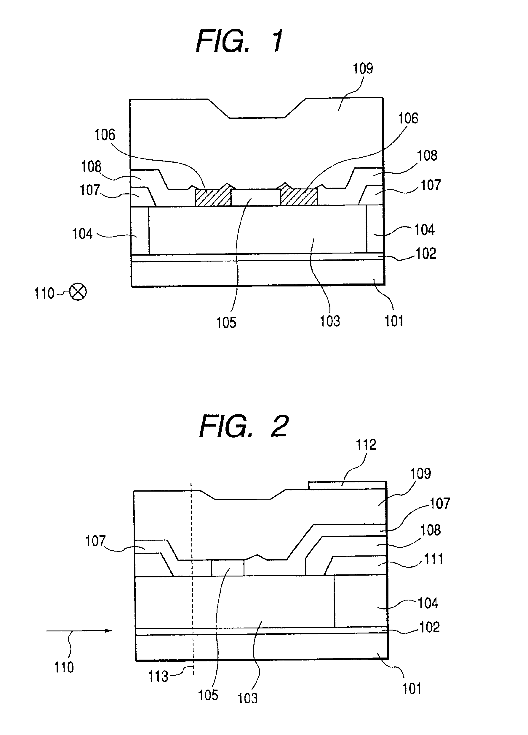
FIGS. 1 and 2 are diagrams showing the structure of a magnetoresistive sensor as one embodiment according to the present invention viewed from the media-opposed surface and section of the plane perpendicular to the depth direction, respectively. Arrow 110 in the drawing denotes the depth direction.

On a substrate 101 is formed a base insulating layer 102, made of, for example, alumina. After subjected to precision polishing by means of chemimechanical polishing (CMP), a lower magnetic shield layer 103 is formed thereon. This is made of Ni8lFe19 having a thickness of 2 μm manufactured by, for example, the sputtering method, the ion beam sputtering method, or the plating method. A resist mask is patterned in a predetermined size in this layer, and other portions thereof are subjected to ion milling to strip off the resist. Al2O3 is grown thereon to fill in portions 104 removed by ion milling. After this is subjected to CMP, an electrode layer made of Cu or Ru (not shown) is grown by 20...

example 2

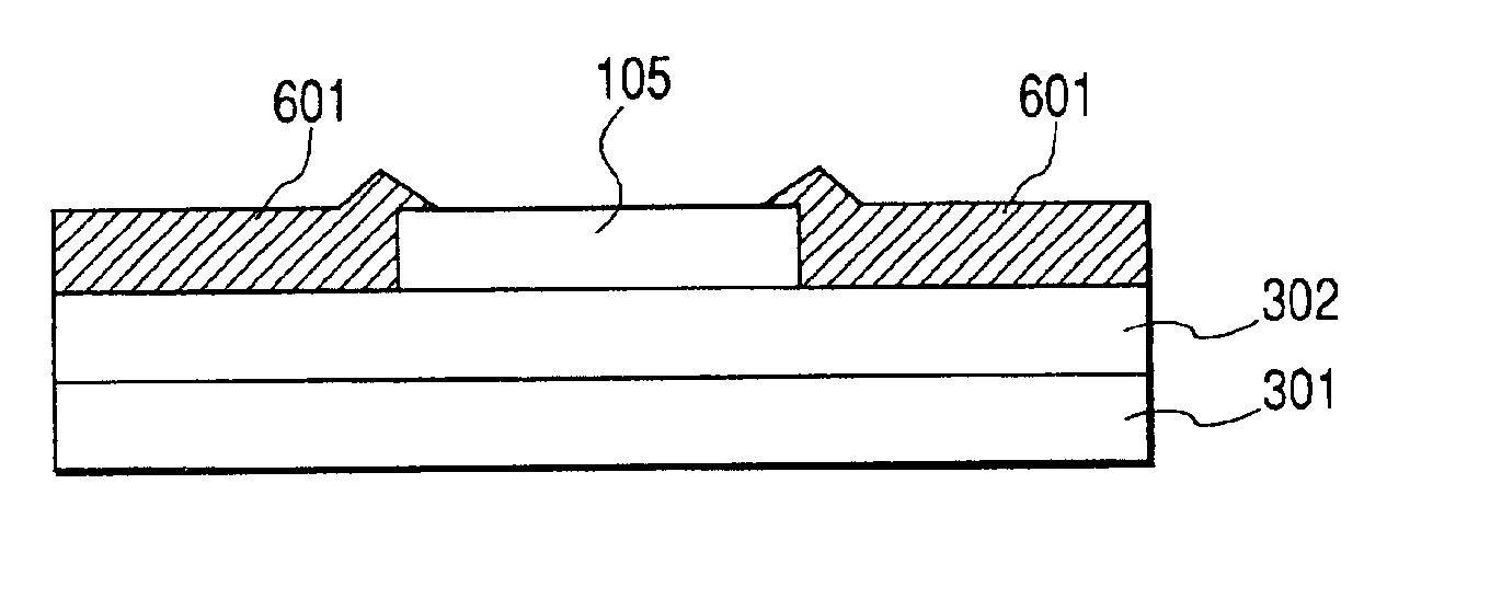
The magnetoresistive sensor in Example (1) described above has the structure by lamination from the lower portion. The structure in which the upper and lower portions are reversed can also give the same effect.

example 3

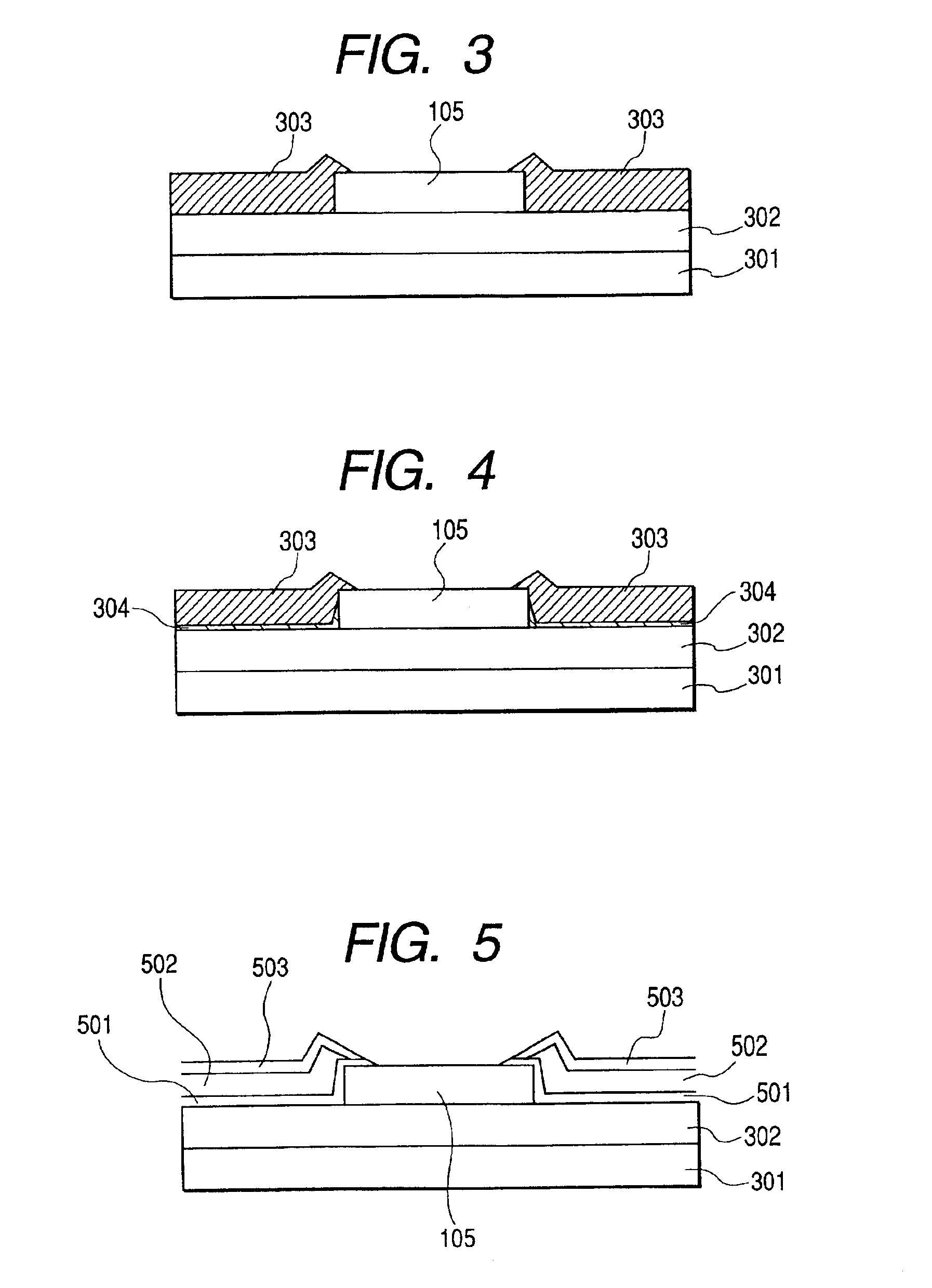
In Example (1) described above, in formation of the magnetic domain control layer using a spinel type oxide such as γ-Fe2O3, on the underlayer 304 of the magnetic domain control layer 303, is formed, in place of the CoO layer, an oxide layer having a crystal structure of NaCl type such as Mg (200), NiO (200), EuO (200), FeO (200) or ZnO (200) as well as a (200) plane. Then, the spinel ferrite formed thereon can be crystallized at low temperature. As a method of forming this layer, there is a method of manufacturing these layers by the sputtering method, the ion beam sputtering method or the cluster ion beam method. As a method other than this, on the lower shied 302 a layer of Co, Mg, Ni, Eu, Fe or Zn is formed in a thickness of 1-5 nm. This layer is exposed to oxygen in vacuum, is irradiated with oxygen using ECR plasma, or is exposed to low-pressure oxygen by heating the substrate (100 to 250° C.) so as to form an oxide layer, thereby forming a spinel ferrite thereon. This method ...


PUM

PropertyMeasurementUnit
temperatureaaaaaaaaaa
thicknessaaaaaaaaaa
thicknessaaaaaaaaaa

Abstract

A magnetoresistive sensor of the type of flowing a signal sensing current perpendicular to the plane to improve resolution at reproducing a signal, a magnetic head using the magnetoresistive sensor, and a magnetic disk apparatus. A magnetoresistive sensor comprising a substrate, a pair of magnetic shield layers consisting of a lower magnetic shield layer and an upper magnetic shield layer, a magnetoresistive sensor layer, disposed between the pair of magnetic shield layers, an electrode terminal for flowing a signal current perpendicular to the plane of the magnetoresistive sensor layer, and magnetic domain control layers for controlling Barkhausen noise of the magnetoresistive sensor layer, wherein the magnetic domain control layers disposed in contact with opposite ends of the magnetoresistive sensor layer consist of a material having high electric resistivity and with a specific resistance not less than 10 mΩcm so as to give the magnetoresistive sensor having excellent reproducing resolution.

Description

BACKGROUND OF THE INVENTION1. Field of the InventionThe present invention relates to a magnetoresistive sensor including magnetic domain control layers for the magnetoresistive sensor for reading back magnetically recorded information, a magnetic head, and a magnetic disk apparatus. More specifically, it relates to a magnetoresistive sensor having excellent reproducing resolution, a magnetic head using the same, and a magnetic disk apparatus.2. Description of the Related ArtThe recording density in a magnetic disk apparatus has been improved significantly, and the demand that the performance of the magnetic read / write heads thereof be enhanced is increased in regard to both characteristics of read and write.Regarding the read head sensor, it is necessary to improve the techniques concerning three points: (1) improvement of a technique for making the efficiency higher, (2) improvement of a technique for making the track width smaller, and (3) a technique for making the gap between th...

Claims


Application Information

Patent Timeline
Patent Type & Authority Patents(United States)
IPC IPC(8): G01R33/06G01R33/09G11B5/39G11B5/127G11B5/33H01L43/08
CPCB82Y10/00B82Y25/00G01R33/09G11B5/3909G11B5/3932G11B5/3967G11B5/3903G11B2005/3996
Inventor TAKAHASHI, HIROMASAARAI, REIKOSOEYA, SUSUMU
Owner HITACHI GLOBAL STORAGE TECH JAPAN LTD
Why Eureka
Try Eureka