Supercharge Your Innovation With Domain-Expert AI Agents!

Probe module and a testing apparatus

a technology of probe module and test apparatus, which is applied in the direction of electrical testing, measurement devices, instruments, etc., can solve the problem of not being able to correspond to the test signal of high frequency accompanying the semiconductor testing apparatus of high speed

Inactive Publication Date: 2005-08-30
ADVANTEST CORP
View PDF5 Cites 72 Cited by
  • Summary
  • Abstract
  • Description
  • Claims
  • Application Information

AI Technical Summary

Benefits of technology

[0013]The first signal transmission pattern may supply a pulse input signal to the device under test, the second signal transmission pattern may supply a direct current input si

Problems solved by technology

In the configuration of the conventional interface part 200, however, there is a practical problem that it cannot correspond to the test signal of high frequency accompanying the semiconductor testing apparatus of high speed because of the length of the wiring between the probe needle 204 and the semiconductor testing apparatus.

Method used


Image

  • Probe module and a testing apparatus
  • Probe module and a testing apparatus
  • Probe module and a testing apparatus

Examples


Embodiment Construction

[0030]The invention will now be described based on the preferred embodiments, which do not intend to limit the scope of the present invention, but exemplify the invention. All of the features and the combinations thereof described in the embodiment are not necessarily essential to the invention.

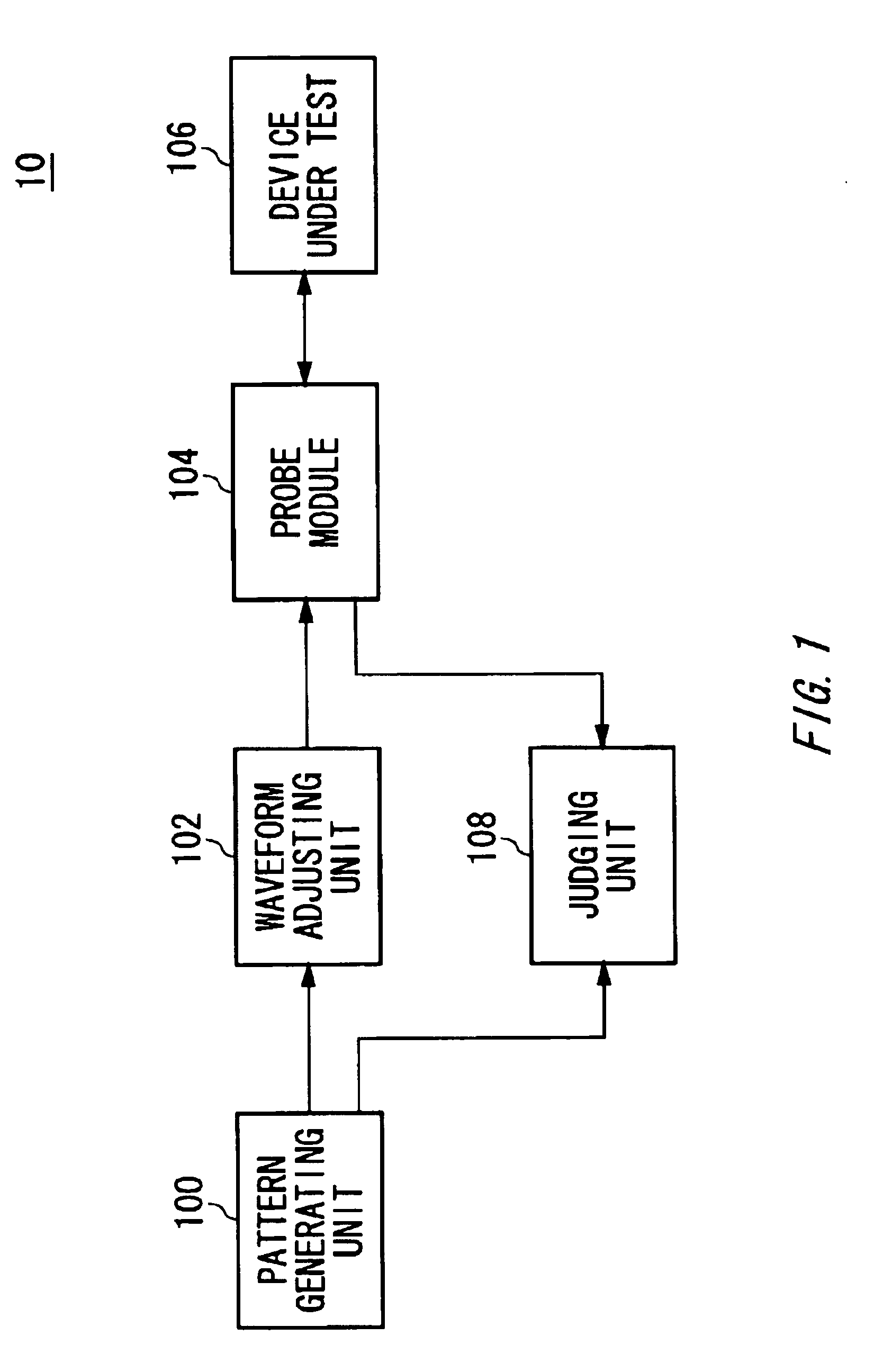
[0031]FIG. 1 shows an example of the configuration of a semiconductor testing apparatus 10 according to the present invention. The semiconductor testing apparatus 10 includes a pattern generating unit 100, a waveform adjusting unit 102, a probe card 50, and a judging unit 108.

[0032]The pattern generating unit 100 generates a test signal to test a device under test 106, and supplies it to the waveform adjusting unit 102.

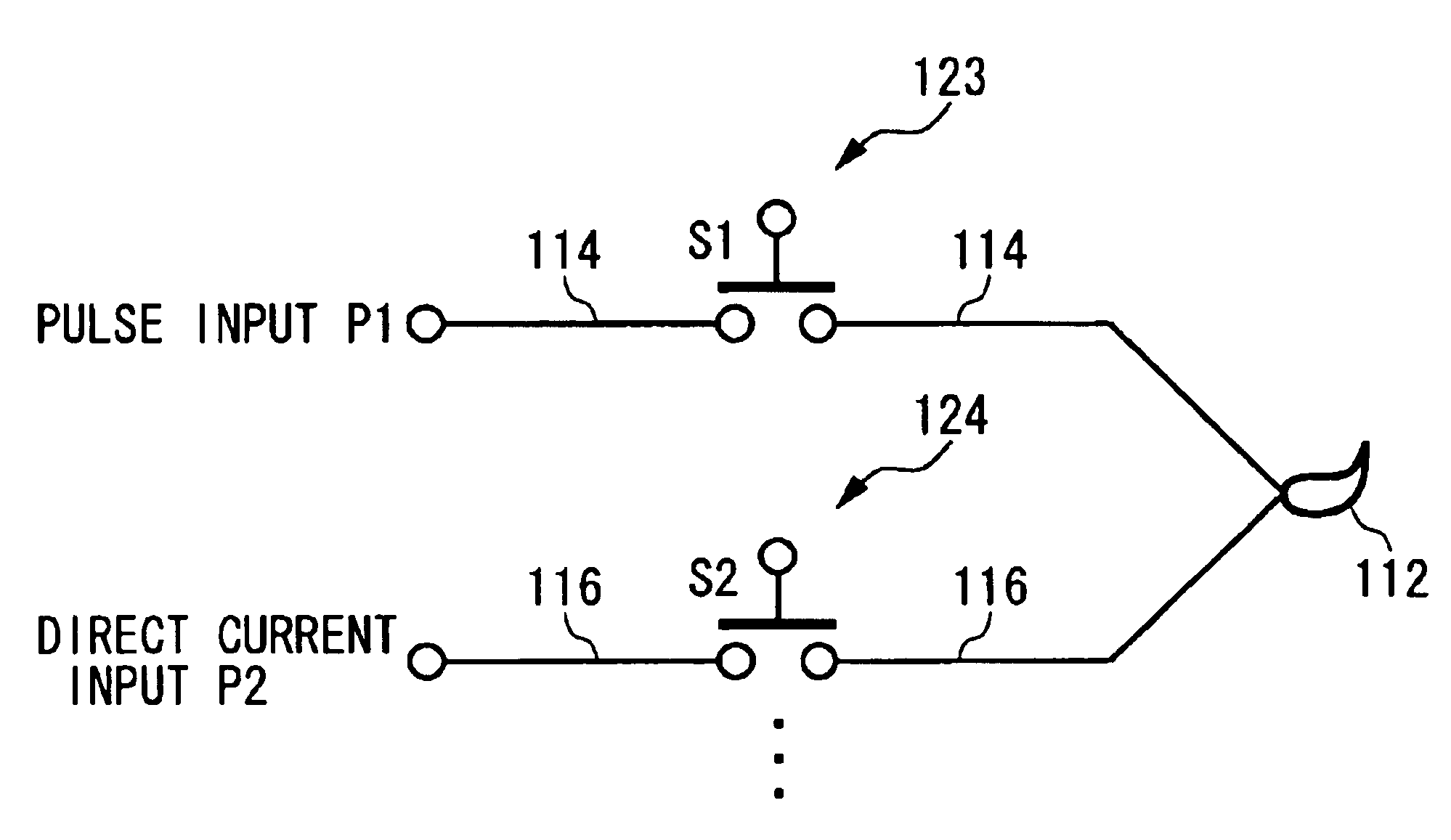
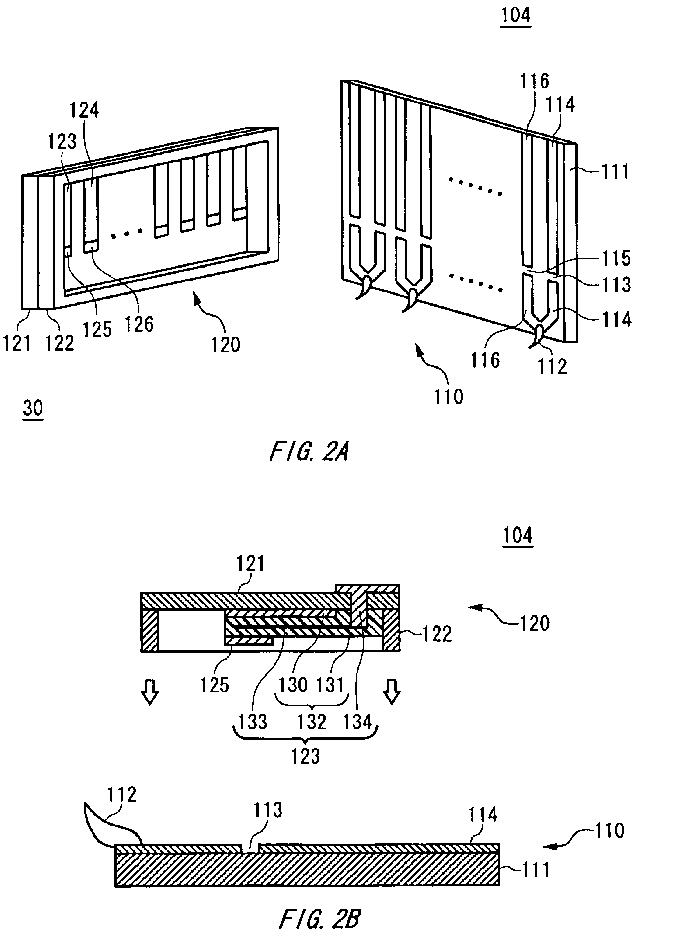
[0033]The waveform adjusting unit 102 adjusts the test signal generated by the pattern generating unit 100, and supplies the adjusted test signal to the probe module 104. The waveform adjusting unit 102 may supply the test signal to the probe module 104 at a desired timing. In ...


PUM


Abstract

A probe module electrically coupled to a terminal of a device under test for sending and / or receiving a signal to and / or from the device under test, includes a first substrate, a probe pin provided on the first substrate to be in contact with the terminal of the device under test, a first signal transmission pattern formed on the first substrate, the first signal transmission pattern being electrically coupled to the probe pin, with a gap formed at the first signal transmission pattern not to transmit any electric signal, and a for short-circuiting or open-circuiting the gap of the first signal transmission pattern.

Description

[0001]The present application is a continuation application of PCT / JP02 / 07410 filed on Jul. 23, 2002 which claims the benefit of, and priority from, a Japanese patent application No. 2001-244161 filed on Aug. 10, 2001, the entire contents of which are incorporated herein by reference for all purposes.BACKGROUND OF THE INVENTION[0002]1. Field of the Invention[0003]The present invention relates to a probe module and a testing apparatus.[0004]2. Related Art[0005]FIGS. 5A and 5B show the configuration of an interface part 200 of a conventional semiconductor testing apparatus for a device under test. The interface part 200 sends and receives electric signals with an IC chip, which is a device under test formed on a wafer 202, at a test head of the semiconductor testing apparatus. FIG. 5A shows a cross-sectional view of the interface part 200 and FIG. 5B shows a circuit of the interface part 200.[0006]As shown in FIG. 5A, the interface part 200 includes a probe needle 204, a probe card 20...

Claims


Application Information

Patent Timeline
IPC IPC(8): G01R1/073
CPCG01R1/07385
Inventor MAEDA, YASUHIROTAKAYANAGI, FUMIKAZU
Owner ADVANTEST CORP
Features
  • R&D
  • Intellectual Property
  • Life Sciences
  • Materials
  • Tech Scout
  • Unparalleled Data Quality
  • Higher Quality Content
  • 60% Fewer Hallucinations
Learn More