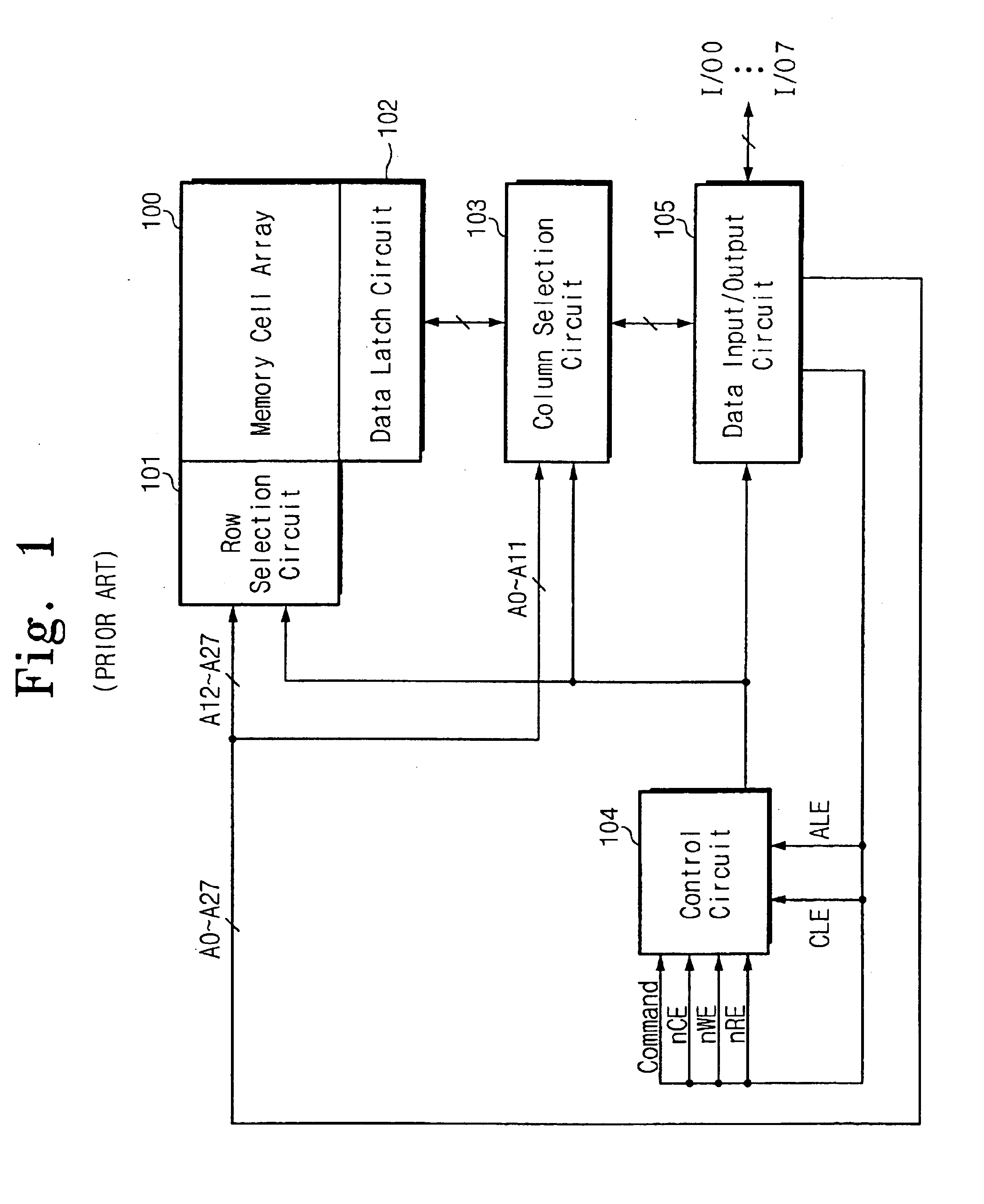
Nonvolatile semiconductor memory with X8/X16 operation mode using address control
a technology of nonvolatile semiconductor memory and address control, which is applied in the field of flash memory, can solve the problems of inefficiency of the fabrication process, and achieve the effect of controlling the data rate operation of the memory
- Summary
- Abstract
- Description
- Claims
- Application Information
AI Technical Summary
Benefits of technology
Problems solved by technology
Method used
Image

Examples
Embodiment Construction
[0033]The present invention may be embodied in different forms and should not be construed as limited to the embodiments set forth herein. Rather, these embodiments are provided so that this disclosure will be thorough and complete, and will fully convey the scope of the invention to those skilled in the art.
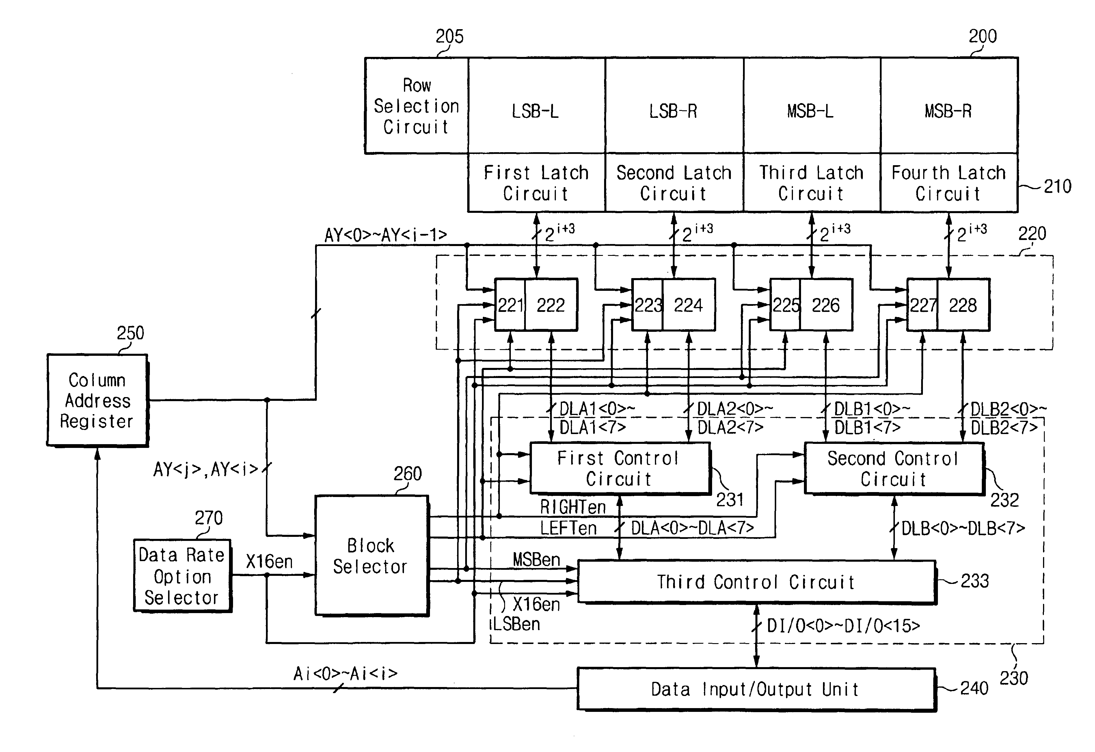
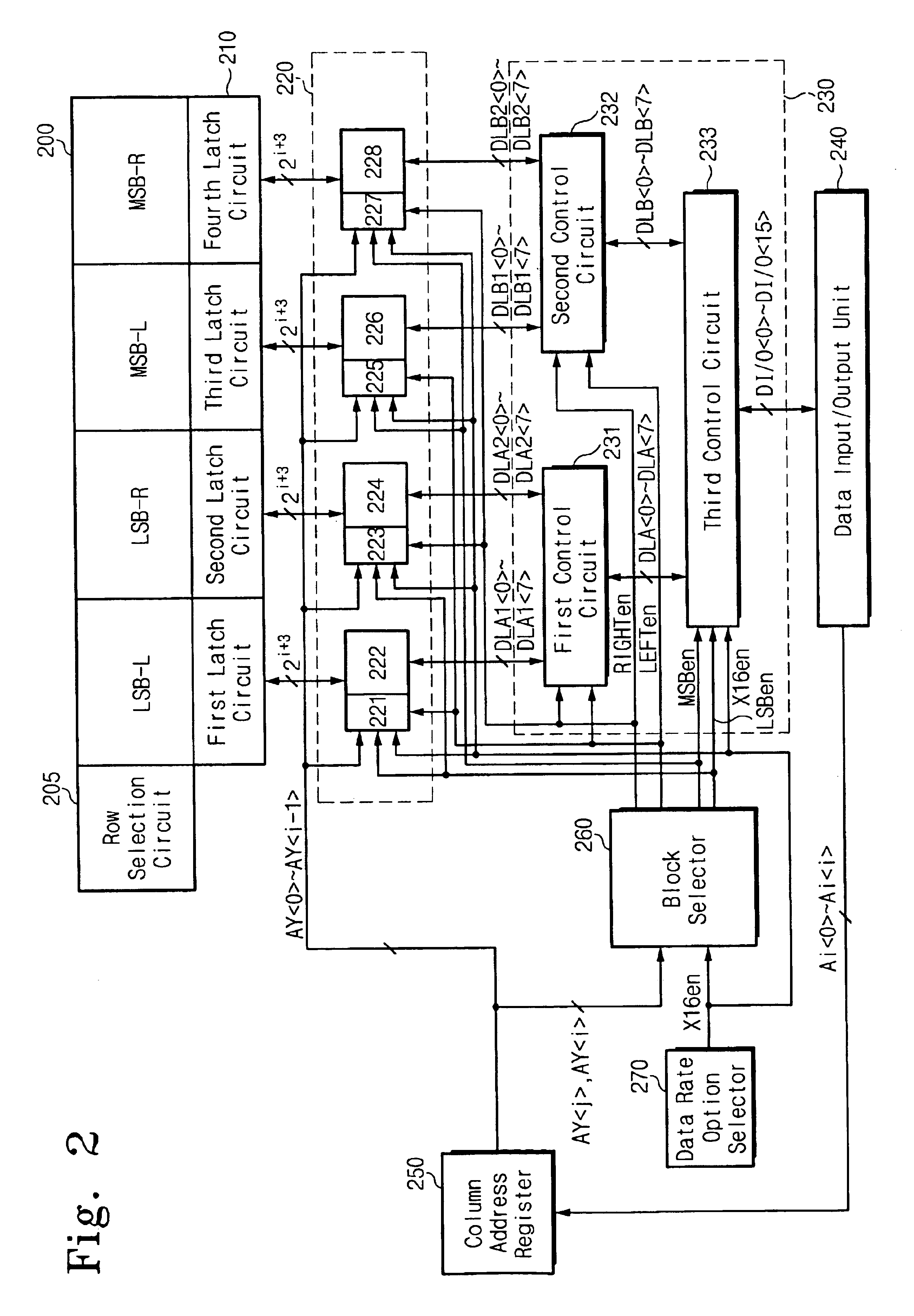
[0034]FIG. 2 is a block diagram showing a NAND type flash memory having input / output of ×8 or ×16 data rate according to a predetermined data rate option.
[0035]The NAND type flash memory comprises a memory cell array 200, a row selection circuit 205, a data latch circuit 210, a data input / output part 240, a column address register 250, a data rate option selector 270, a block selector 260, a column selection circuit 220 and a data input / output controller 230. The memory cell array 200 comprises total four blocks LSB-L, LSB-R, MSB-L and MSB-R. The row selection circuit 205 is for selecting a row of the memory cell array 200. The data latch circuit 210 includes First-Fourth latchi...
PUM
 Abstract
Description
Claims
Application Information
 - R&D
- Intellectual Property
- Life Sciences
- Materials
- Tech Scout
- Unparalleled Data Quality
- Higher Quality Content
- 60% Fewer Hallucinations
Browse by: Latest US Patents, China's latest patents, Technical Efficacy Thesaurus, Application Domain, Technology Topic, Popular Technical Reports.
© 2025 PatSnap. All rights reserved.Legal|Privacy policy|Modern Slavery Act Transparency Statement|Sitemap|About US| Contact US: help@patsnap.com