RF device and communication apparatus using the same

a communication apparatus and rf technology, applied in the field of rf devices, can solve the problems of high loss as a filter, large low relative dielectric constant, and insufficient increase of quality factor, and achieve the effect of low filter loss

Inactive Publication Date: 2006-01-10
PANASONIC CORP
View PDF19 Cites 50 Cited by
  • Summary
  • Abstract
  • Description
  • Claims
  • Application Information

AI Technical Summary

Benefits of technology

[0020]In view of the above described problems, an object of this invention is to provide an RF device having a low filter loss and not suffering from a problem about a line impedance, or a compact RF device not suffering from a problem about a line impedance.

Problems solved by technology

However, the first conventional RF device configured as described above, the transmitting filter 1206 and the receiving filter 1027 are composed of an inductor or capacitor with a low Quality factor, and therefore, have a high loss as a filter.
Furthermore, the microstrip resonator structure for increasing the Quality factor has a problem in that the RF device including the substrate 1101 made of a low temperature cofired ceramic with low relative dielectric constant becomes quite large because the size of the resonator is inversely proportional to the frequency and the square root of the relative dielectric constant.
Even with the microstrip resonator structure, since it is also affected by the substrate 1101 with low relative dielectric constant, the Quality factor cannot be increased sufficiently, and for example, a circuit provided for the CDMA mode still has a problem of the filter loss.
In the second conventional RF device configured as described above, if a line is provided thereon or therein, the impedance of the line is increased because the substrates constituting the RF multilayered device are made of a low temperature cofired ceramic with high relative dielectric constant, and thus, it is quite difficult to form a complicated circuit in each substrate.
In addition, it is also quite difficult to implement a discrete component, such as a discrete resistor, a discrete capacitor, a discrete inductor and a packaged semiconductor, on the second conventional RF device, because the line impedance of the discrete component itself is increased.

Method used


Image

  • RF device and communication apparatus using the same
  • RF device and communication apparatus using the same
  • RF device and communication apparatus using the same

Examples


embodiment 1

[0152](Embodiment 1)

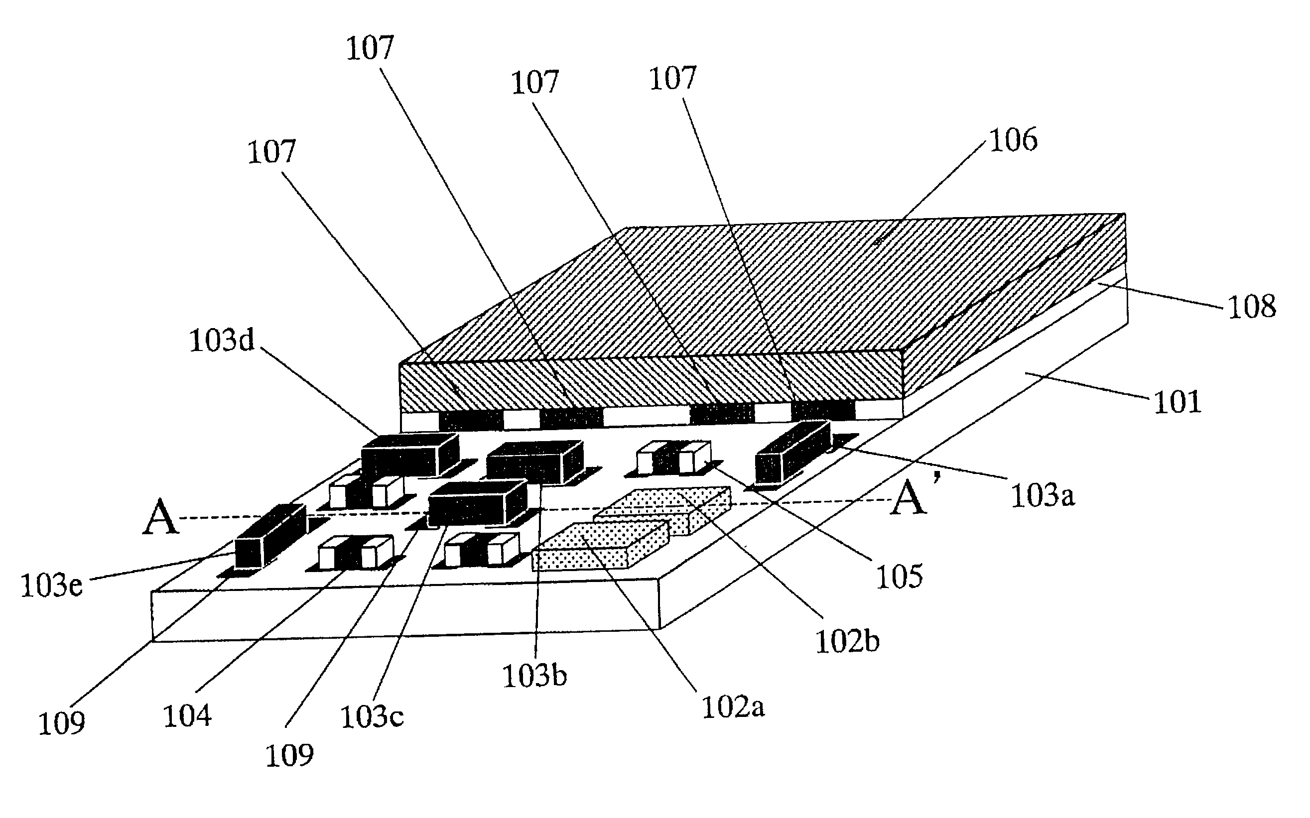
[0153]FIG. 1 is a perspective view of an RF device according to an embodiment 1 of this invention. A substrate 101 is an example of a first substrate according to this invention, which is made of a low temperature cofired ceramic with low dielectric constant (hereinafter, “low dielectric constant” means a lower relative dielectric constant) Reference numerals 102a and 102b denote a SAW filter, reference numerals 103a to 103e denote a PIN diode, which is one example of a semiconductor device according to this invention, reference numeral 104 denotes a discrete inductor, reference numeral 105 denotes a discrete capacitor, and a substrate 106 is an example of a second substrate according to this invention, which is made of a high temperature cofired ceramic with high dielectric constant (hereinafter, “high dielectric constant” means a higher relative dielectric constant). A metal foil resonator 107 is one example of a part of a resonator according to this invention....

embodiment 2

[0190](Embodiment 2)

[0191]Now, an RF device according to a second embodiment of this invention will be described with reference to the drawings.

[0192]FIG. 9 is a circuit diagram of the RF device according to the embodiment 2 of this invention. In FIG. 9, reference numerals 501 to 505 denote a metal foil resonator serving as the quarter-wavelength tip-short-circuited resonator, reference numerals 506, 507 denote a series capacitor, reference numerals 508, 509 denote a ground capacitor, reference numerals 510 to 512 denote a coupling inductor, reference numerals 513, 154 denote a coupling capacitor, reference numerals 515, 516 denote a bypass capacitor, reference numeral 517 denotes a capacitor for matching between terminals, reference numeral 518 denotes an inductor for matching between terminals, reference numerals 519 to 523 denotes a switch, reference numerals 524 to 528 denote a switch coupling capacitor, reference numeral 529 denotes an antenna terminal, reference numeral 530 de...


PUM


Abstract

An RF device includes a first substrate having a lower relative dielectric constant, a first RF circuit for a lower frequency band provided in the first substrate, a second substrate having a higher relative dielectric constant larger than the lower relative dielectric constant, and a second RF circuit for a higher frequency band having a part of the second RF circuit sandwiched between the first substrate and the second substrate. The first RF circuit and the second RF circuit are connected to each other and the second substrate is partially overlaid on the first substrate. A semiconductor device or passive device is provided on a region in the surface of the first substrate on which the second substrate is not overlaid, and a multilayered wiring pattern made of copper or silver is formed in the first substrate to form the first RF circuit.

Description

BACKGROUND OF THE INVENTION[0001]1. Field of the Invention[0002]The present invention relates to an RF device mainly used in a high frequency radio apparatus, such as a cellular phone.[0003]2. Related Art of the Invention[0004]Recently, as mobile communication users have been increased and a system therefor has become global, an RF device has become a focus of attention that enables the EGSM, DCS and UMTS systems provided for respective frequencies shown in FIG. 18 to be used with one cellular phone. With reference to drawings, a first conventional RF device will be described below.[0005]FIG. 19 is a cross-sectional view of the first conventional RF device. In FIG. 19, reference numeral 1101 denotes a low temperature cofired ceramic body with a low relative dielectric constant. Reference numeral 1102 denotes a multilayered wiring conductor for constituting part of an RF circuit. Reference numeral 1103 denotes an interlayer via hole and reference numeral 1104 denotes a discrete compo...

Claims


Application Information

Patent Timeline
Patent Type & Authority Patents(United States)
IPC IPC(8): H04B1/28H01P1/15H01P1/203H01P1/213
CPCH01P1/15H01P1/213H01P1/20345
Inventor YAMAKAWA, TAKEHIKOYAMADA, TORUISHIZAKI, TOSHIO
Owner PANASONIC CORP
Why Eureka
Try Eureka