Semiconductor device

a technology of electromagnetic wave shielding and semiconductor devices, applied in the direction of basic electric elements, telemetry/telecontrol selection arrangements, radio control devices, etc., can solve the problems of increasing the number of processes required to cover the device with the shield casing, the cost of the shield casing itself, and the noise of the electromagnetic wave shielding. , to achieve the effect of sufficient effective electromagnetic wave shielding, and greater degree of mounting freedom

Active Publication Date: 2006-03-07
SHARP KK
View PDF9 Cites 22 Cited by
  • Summary
  • Abstract
  • Description
  • Claims
  • Application Information

AI Technical Summary

Benefits of technology

[0012]Accordingly, an object of the present invention is to provide a semiconductor device which is capable of obtaining a sufficient electromagnetic shielding effect, which is small and low-cost, and which has a high degree of mounting freedom on a board.

Problems solved by technology

Accordingly, the semiconductor device for optical communication is very sensitive to noise.
(a) There is an increase in the number of processes required for covering the device with the shield casing.
(b) There is a cost for the shield casing itself.
(c) There is a restriction on the mounting freedom of the semiconductor device on the board, which is dependent on the design of the shield casing.
In the conventional example, however, the electrical contact between the lead frame and the conductive resin tends to be insufficient, and consequently the shielding effect also tends to be insufficient, disadvantageously.

Method used


Image

  • Semiconductor device
  • Semiconductor device
  • Semiconductor device

Examples


first embodiment

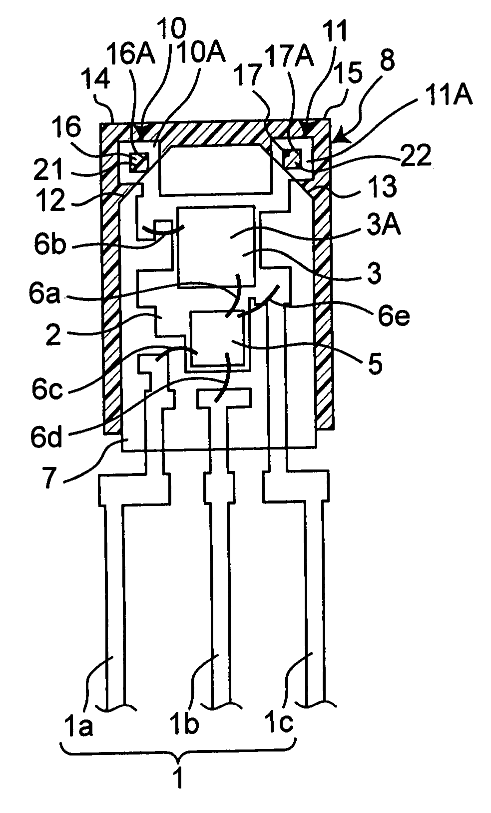
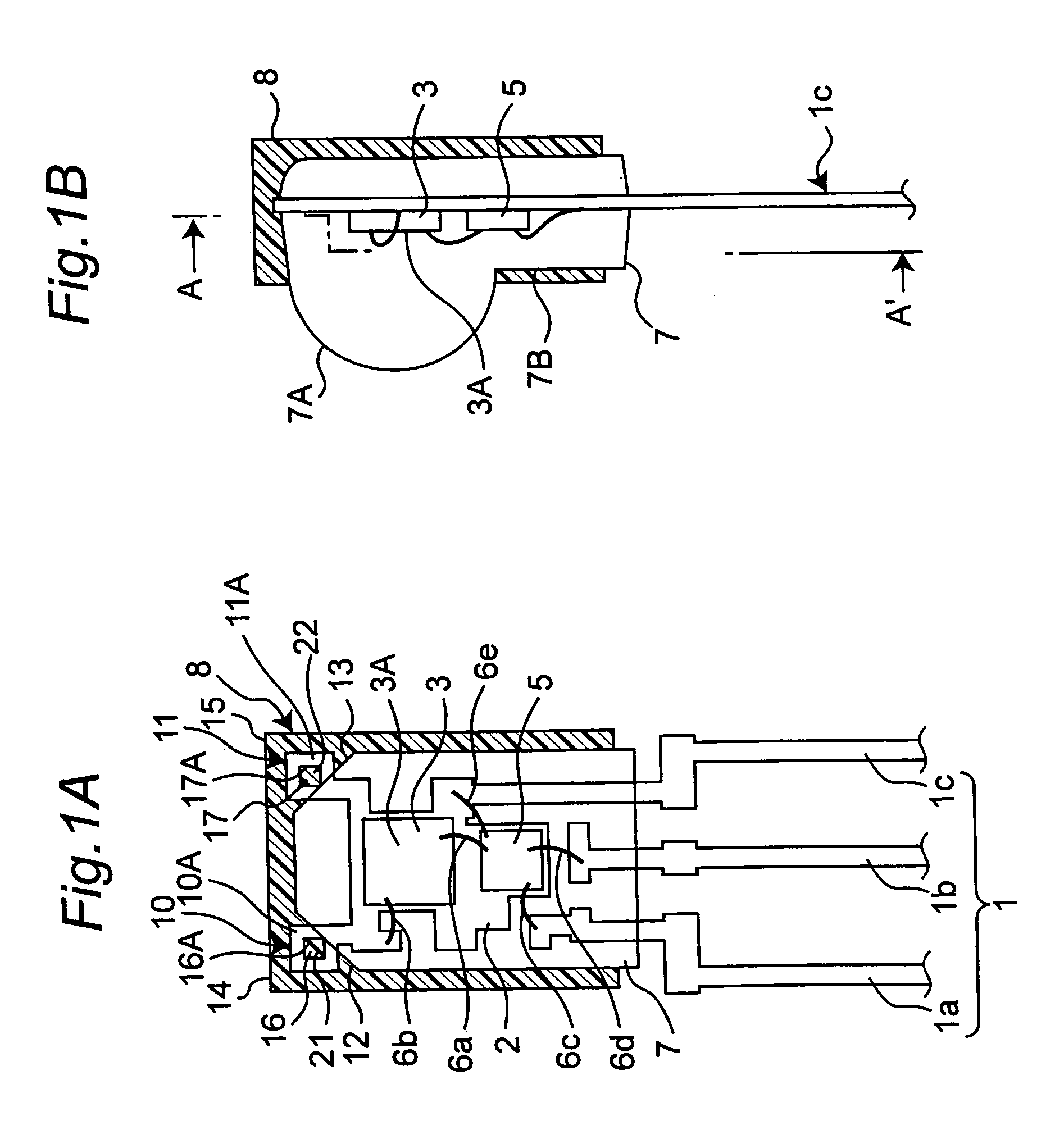
[0048](First Embodiment)

[0049]FIG. 1A and FIG. 1B show the semiconductor device for optical communication as the first embodiment of the invention. FIG. 1A is a cross sectional view taken along line A–A′ of FIG. 1B.

[0050]The semiconductor device of the first embodiment is provided with a lead frame 1, which is composed of a first lead 1a for signal, a second lead 1b for power source and a third lead 1c for grounding. The semiconductor device is also provided with a light-receiving chip 3, which is a photodetector mounted on a mount portion 2 of the third lead 1c for grounding, and a control IC chip 5 which is a signal processing section. The light-receiving chip 3 is implemented by a photodiode or a phototransistor or the like. The control IC chip 5 incorporates a high-gain amplifier.

[0051]The control IC chip 5 is connected to the light-receiving chip 3 by a conductive wire 6a, and the light-receiving chip 3 is connected to the third lead 1c by a conductive wire 6b. In addition, the...

second embodiment

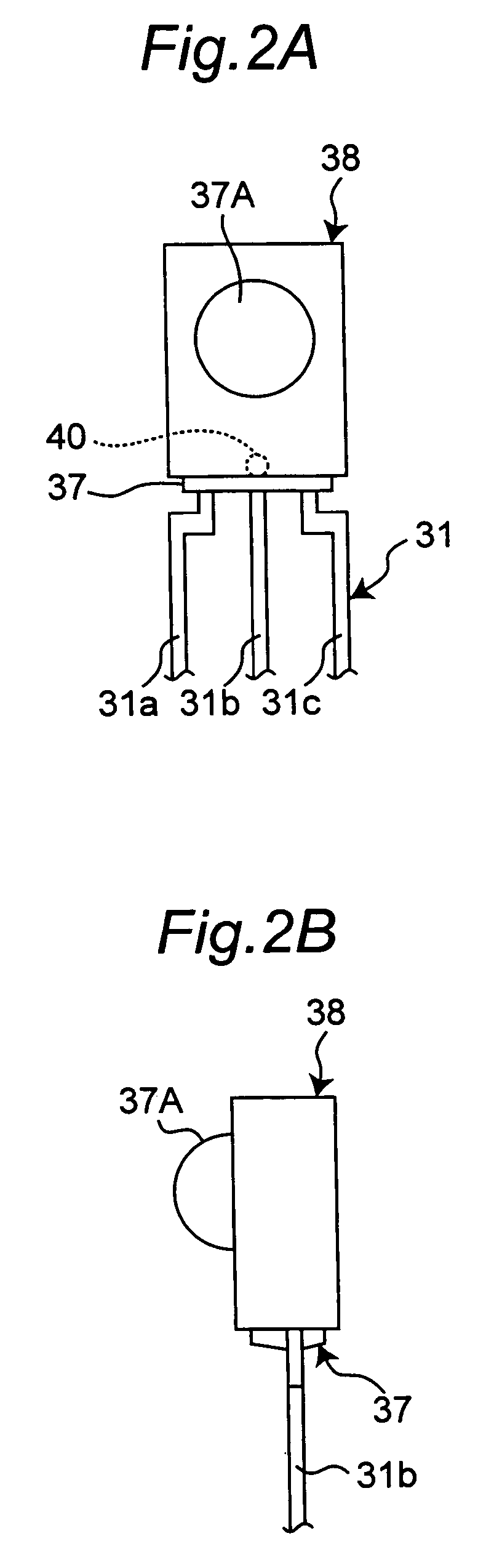
[0059](Second Embodiment)

[0060]FIG. 2 and FIG. 3 show a second embodiment of the semiconductor device for optical communication according to the present invention. FIG. 2A shows an external front view and FIG. 2B shows a side view of the second embodiment of the present invention. FIG. 3A is a cross-sectional view taken along line A–A′ of FIG. 3B.

[0061]The semiconductor device according to the second embodiment is provided with a lead frame 31, which is composed of first lead 31a for signal, second lead 31b for grounding, and third lead 31c for power source. The semiconductor device is also provided with a light-receiving chip 33 which is a photodetector mounted on a mount portion 32 of the second lead 31b for grounding, and a control IC chip 35 which is a signal processing section. The control IC chip 35 is connected to the light-receiving chip 33 by a conductive wire 36a, and the light-receiving chip 33 is connected to the second lead 31b by a conductive wire 36b. In addition, the...

third embodiment

[0068](Third Embodiment)

[0069]FIG. 4 and FIG. 5 show a third embodiment of the semiconductor device for optical communication according to the present invention. FIG. 4A shows an external front view and FIG. 4B shows a sectional view of the third embodiment of the present invention. FIG. 5A is a cross-sectional view taken along line A–A′ of FIG. 5B. The semiconductor device of the third embodiment has the same structure as the semiconductor device of the second embodiment except the following point (i).

[0070](i) The first seal portion 37 is provided with a fill hole 44 of which peripheral surface 44A is of a rectangular-columnar shape, instead of a fill hole 40 of which inner peripheral surface is cylindrical, and the fill hole 44 is filled with a rectangular-columnar conductive portion 45 of the second seal portion 38.

[0071]In the third embodiment, the fill hole 44 provided for the first seal portion 37 is of a rectangular-columnar shape, so that the mechanical strength of coupling...


PUM


Abstract

A semiconductor device allows a second seal portion 8 made of a conductive resin to function as an electromagnetic wave shield for a photodetector 3 and a control IC chip 5 sealed with a first seal portion 7 made of a light-transmitting resin, when a third lead 1c for grounding of a lead frame 1 is connected to a ground terminal on a board. Conductive portions 21, 22 of the second seal portion 8 fill through holes 16, 17 provided for projecting portions 10, 11 of the lead frame 1 so as to be in close contact with peripheral surfaces 16A, 17A of the through holes 16, 17. The through holes 16, 17 have peripheral surfaces 16A, 17A of a rectangular-columnar shape. The semiconductor device is capable of obtaining a sufficient electromagnetic shielding effect, while it is small and low-cost, having a high degree of mounting freedom on a board.

Description

[0001]This Nonprovisional application claims priority under 35 U.S.C. §119(a) on Patent Application No. P2003-308423 filed in Japan on Sep. 1, 2003, the entire contents of which are hereby incorporated by reference.BACKGROUND OF THE INVENTION[0002]The present invention relates to semiconductor devices provided with a photodetector and a signal processing section, more particularly to a semiconductor device for optical communication which receives an infrared signal from a transmitter and outputs a control signal for controlling operation of each electronic device, on which the semiconductor device is mounted, such as a television receiver, a video tape recorder, an audio component unit and an air conditioner.[0003]Conventionally, a semiconductor device for optical communication has been provided with a light-receiving chip and a control IC chip on a board, some of these chips being sealed with an infrared-transparent resin.[0004]This semiconductor device for optical communication re...

Claims


Application Information

Patent Timeline
Patent Type & Authority Patents(United States)
IPC IPC(8): H01L27/14H01L31/00H01L31/0203H01L31/0232H01L23/29H01J17/18H01L23/00H01L23/28H01L23/31H01L23/48H01L25/16H01L27/146H01L31/0216H04Q9/00
CPCH01L25/167H01L31/0203H01L27/14618H01L2224/48137H01L2224/48247H01L2224/48257H01L2924/3025H01L2924/1815H01L2224/48091H01L2924/00014H01L2924/00H01L2924/181H01L2924/00012
Inventor HONBOH, MASAHIRO
Owner SHARP KK
Why Eureka
Try Eureka