Phase multiplier circuit

a phase multiplier and circuit technology, applied in the direction of generating/distributing signals, pulse techniques, instruments, etc., can solve the problem of difficult to achieve equal spacing

Inactive Publication Date: 2006-03-07
FIEDLER ALAN
View PDF3 Cites 11 Cited by
  • Summary
  • Abstract
  • Description
  • Claims
  • Application Information

AI Technical Summary

Benefits of technology

[0008]The particular utility and value in this phase multiplier circuit is the use of circuitry to measure, and feedback to control, the phases of the output signals such that they are accurately and evenly spaced between 0 and 360 degrees. Small (and, therefore, low-power but poorly-matched) transistors are used to generate a delay from each output signal to the next, and relatively large (and, therefore, well-matched) transistors operating at low power are used to measure the relative phases of the generated signals. This approach simultaneously achieves the desirable goals of both accurate phase control and low power.

Problems solved by technology

These two requirements to achieve equal spacing can be difficult to meet.

Method used


Image

  • Phase multiplier circuit
  • Phase multiplier circuit
  • Phase multiplier circuit

Examples


Embodiment Construction

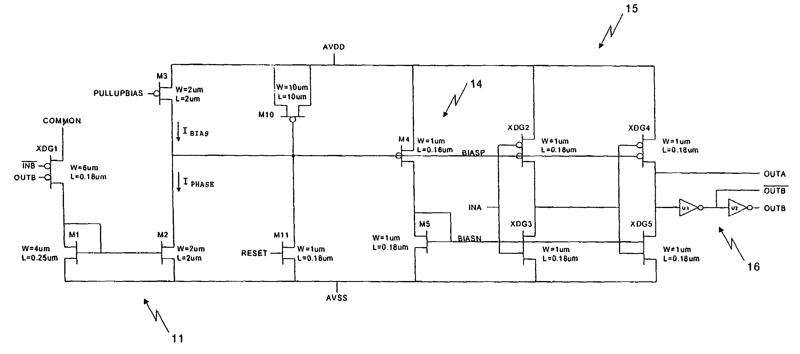
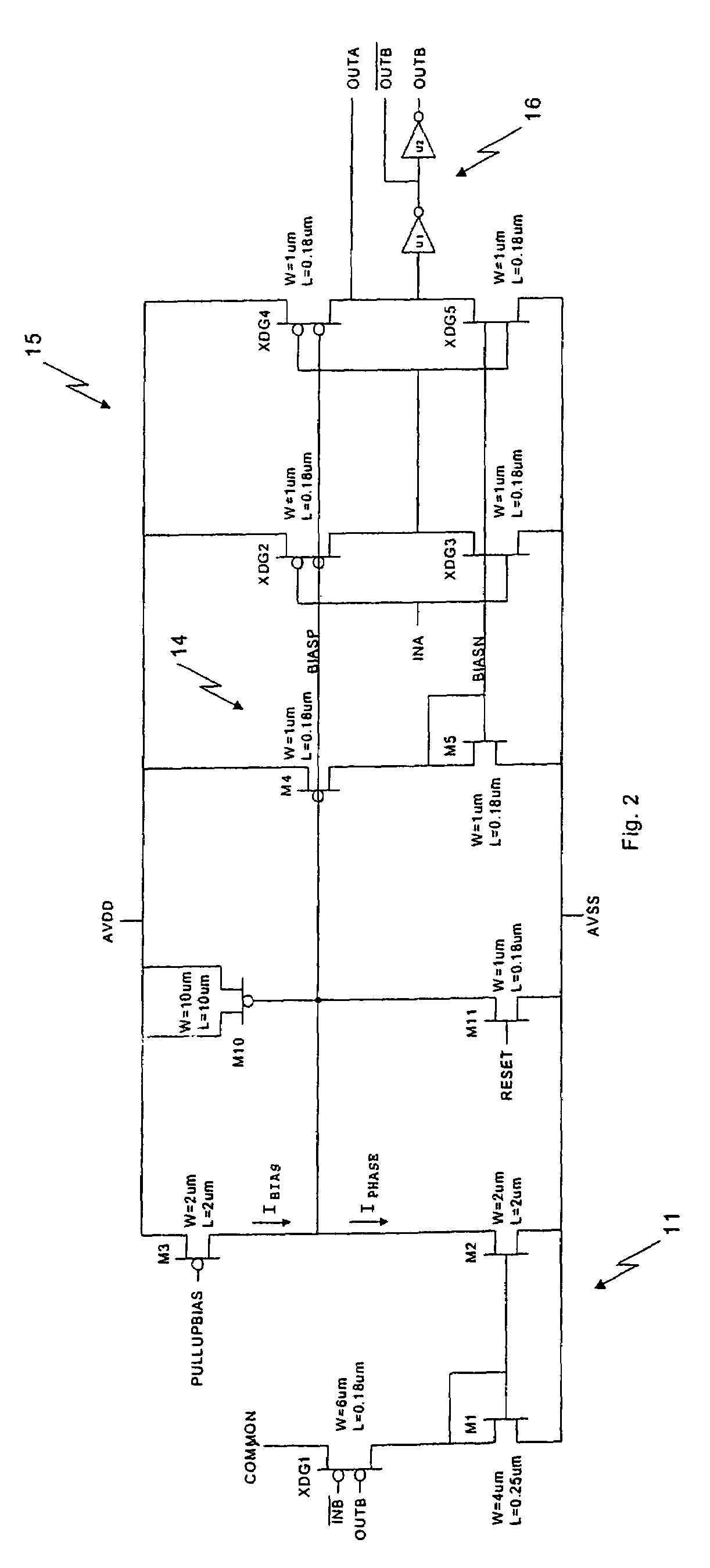
[0017]Three instances of the phase multiplier subcircuit of FIG. 2 and additional circuitry comprise the phase multiplier circuit of FIG. 3. The phase multiplier subcircuit of FIG. 2 comprises a difference circuit 11, a loop filter transistor M10, a reset transistor M11, a BIASN generation circuit 14, a voltage controlled delayed circuit 15, and a buffer 16.

[0018]The difference circuit 11 converts a phase delay to a phase current and subtracts this phase current from a bias current. Difference circuit 11 comprises p-channel dual-gate transistor XDG1 having a source coupled to common node COMMON, and first and second gate inputs coupled to inputs / INB and OUTB; a first current mirror comprising n-channel transistors M1 and M2, and bias current source transistor M3. Transistor XDG1 sources a first current during a period of time when inputs / INB and OUTB are both low, and this period of time is a measure of a phase delay from a falling edge of / INB to a rising edge of OUTB. The first ...


PUM


Abstract

So as to generate multiple output signals whose phases are evenly spaced about 360 degrees, and having a frequency equal to that of an input signal, a phase multiplier circuit includes three or more instances of a phase multiplier subcircuit and additional circuitry configured in a negative feedback loop. Each phase multiplier subcircuit includes a difference circuit, a loop filter transistor, and a voltage-controlled delay circuit. The difference circuit converts to a phase current a delay from an input signal to the delay circuit to an output signal from the delay circuit, and subtracts from the phase current a bias current proportional to the smallest positive delay from the output signal with the largest phase to the output signal with the smallest phase. The subtracted current is integrated by the loop filter transistor, and steady-state operation is achieved when for each phase multiplier subcircuit, the bias current is equal to the phase current. Evenly spaced phases of the output signals about 360 degrees are achieved when the delay to phase current gain and delay to bias current gain are substantially equal.

Description

RELATED APPLICATION[0001]This application claims the benefit of priority pursuant to 35 USC § 119(e) from U.S. provisional patent application Ser. No. 60 / 445,657, filed Feb. 7, 2003, and entirely incorporated herein by reference.BACKGROUND OF THE INVENTION[0002]The function of a phase multiplier circuit is to generate equal-frequency output signals, each having a phase, from an input signal. In one embodiment, the phases of the output signals are evenly spaced between 0 and 360 degrees.[0003]FIG. 1 is a schematic diagram illustrating an example of a phase multiplier of the prior art. This circuit is commonly referred to as a delay-locked loop. A voltage-controlled delay line 2 is coupled to an input signal IN and is comprised of five voltage-controlled delay subcircuits U1, U2, U3, U4, and U5, and has four outputs: OUT1, OUT2, OUT3, and OUT4.[0004]Also included in FIG. 1 is a phase detector 3, a charge pump 4, a loop filter capacitor C1, a reset transistor M3, a reset inverter U12, ...

Claims


Application Information

Patent Timeline
Patent Type & Authority Patents(United States)
IPC IPC(8): H03K3/00G11C8/00H03K5/00H03K5/15H03L7/081
CPCH03K5/1504H03L7/0812H03K2005/00286
Inventor FIEDLER, ALAN
Owner FIEDLER ALAN
Why Eureka
Try Eureka