Semiconductor wafer boat for a vertical furnace

a vertical furnace and semiconductor technology, applied in the direction of charging supports, furnaces, lighting and heating apparatus, etc., can solve the problems of slipping, affecting the manufacture of devices, and introducing contaminants into the device areas of the wafer,

Active Publication Date: 2006-04-25
GLOBALWAFERS CO LTD
View PDF18 Cites 62 Cited by
  • Summary
  • Abstract
  • Description
  • Claims
  • Application Information

AI Technical Summary

Benefits of technology

[0008]In one aspect of the present invention, a wafer boat for use in heat treatment of semiconductor wafers in a vertical furnace generally comprises support rods disposed in fixed arrangement relative to each other. The support rods extend vertically when the wafer boat is placed in the vertical furnace. Fingers are supported by the support rods and extend from the rods. The fingers are arranged in groups lying generally in different common horizontal planes along the vertical extent of the support rods. Wafer holder platforms are adapted to be supported by respective groups of fingers generally at different ones of the horizontal planes. The fingers are adapted to underlie the wafer holder platforms and support the platforms at support locations. The wafer holder platforms are sized and shaped for receiving one of the semiconductor wafers thereon. The fingers and the wafer holder platforms each have a respective first overall maximum thickness. The support location of each of at least one of the fingers and the wafer holder platforms has a second maximum thickness less than the first overall maximum thickness.

Problems solved by technology

If the silicon wafers are not adequately supported during heat treatment, the wafers may undergo slip due to local gravitational and thermal stresses.
As is well known in the art, slip may introduce contaminants into the device areas of the wafers.
Moreover, excessive slip may lead to plastic deformation of the wafers, which in turn may lead to production problems, such as photolithography overlay failures causing yield losses in device manufacture.
Even with the use of wafer holder platforms, however, the 300 mm wafers may undergo slip and plastic deformation if the fingers and wafer holder platforms are not properly constructed.
Unless the fingers and wafer holder platforms remain mechanically stable during heat treatment, they may undergo plastic deformation causing the wafers to undergo slip possibly leading to plastic deformation.
However, increasing the thickness of each finger and the thickness of each wafer holder platform decreases the number of wafers the boat can hold because of dimensional constraints imposed on the boat.
Additionally, thicker fingers and wafer holder platforms increase the thermal mass of the wafer boat which can also be detrimental to the slip performance of the boat.
However, the positions of the fingers relative to the wafers are constrained by dimensional constraints of the boat.

Method used


Image

  • Semiconductor wafer boat for a vertical furnace
  • Semiconductor wafer boat for a vertical furnace
  • Semiconductor wafer boat for a vertical furnace

Examples


Embodiment Construction

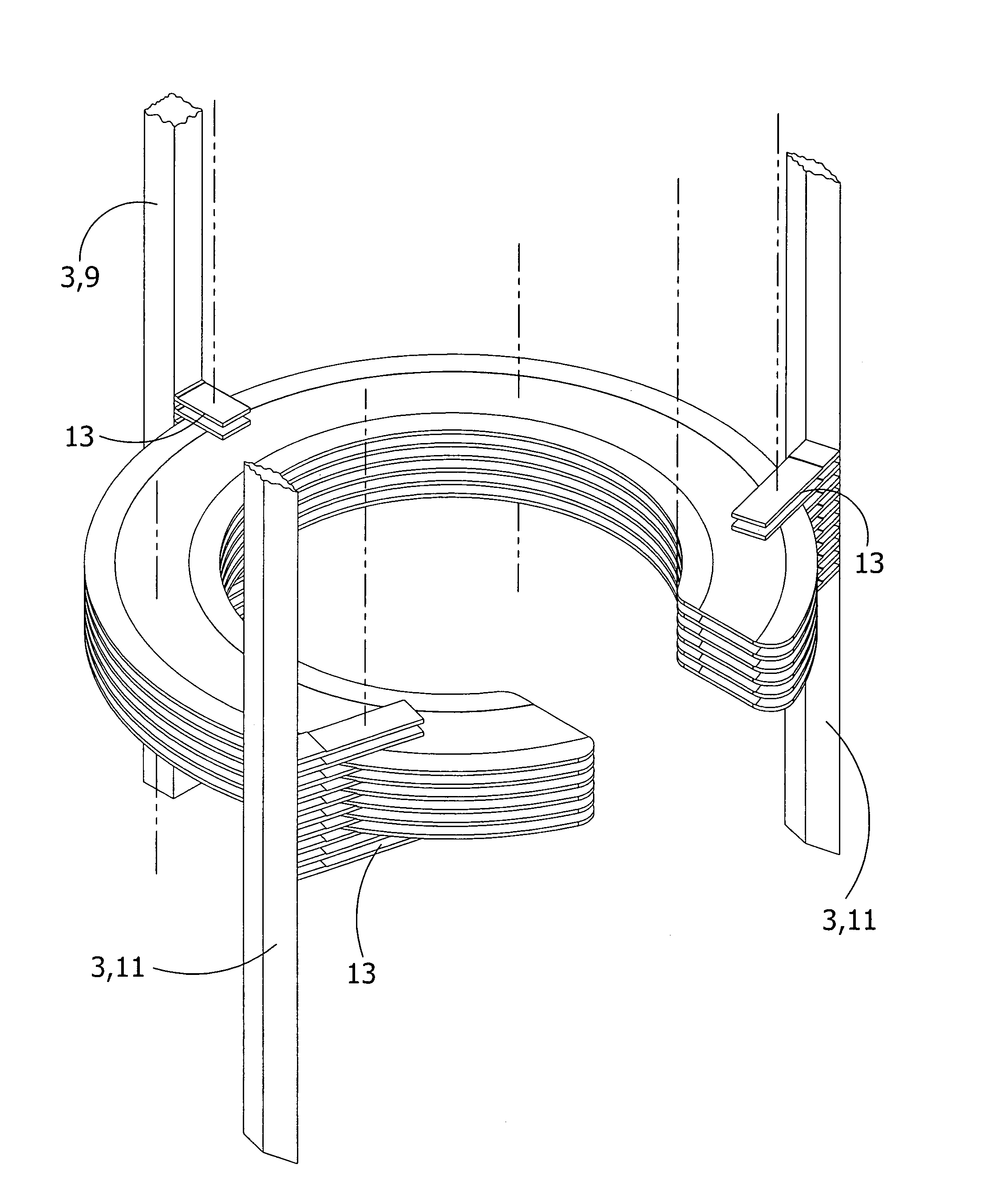
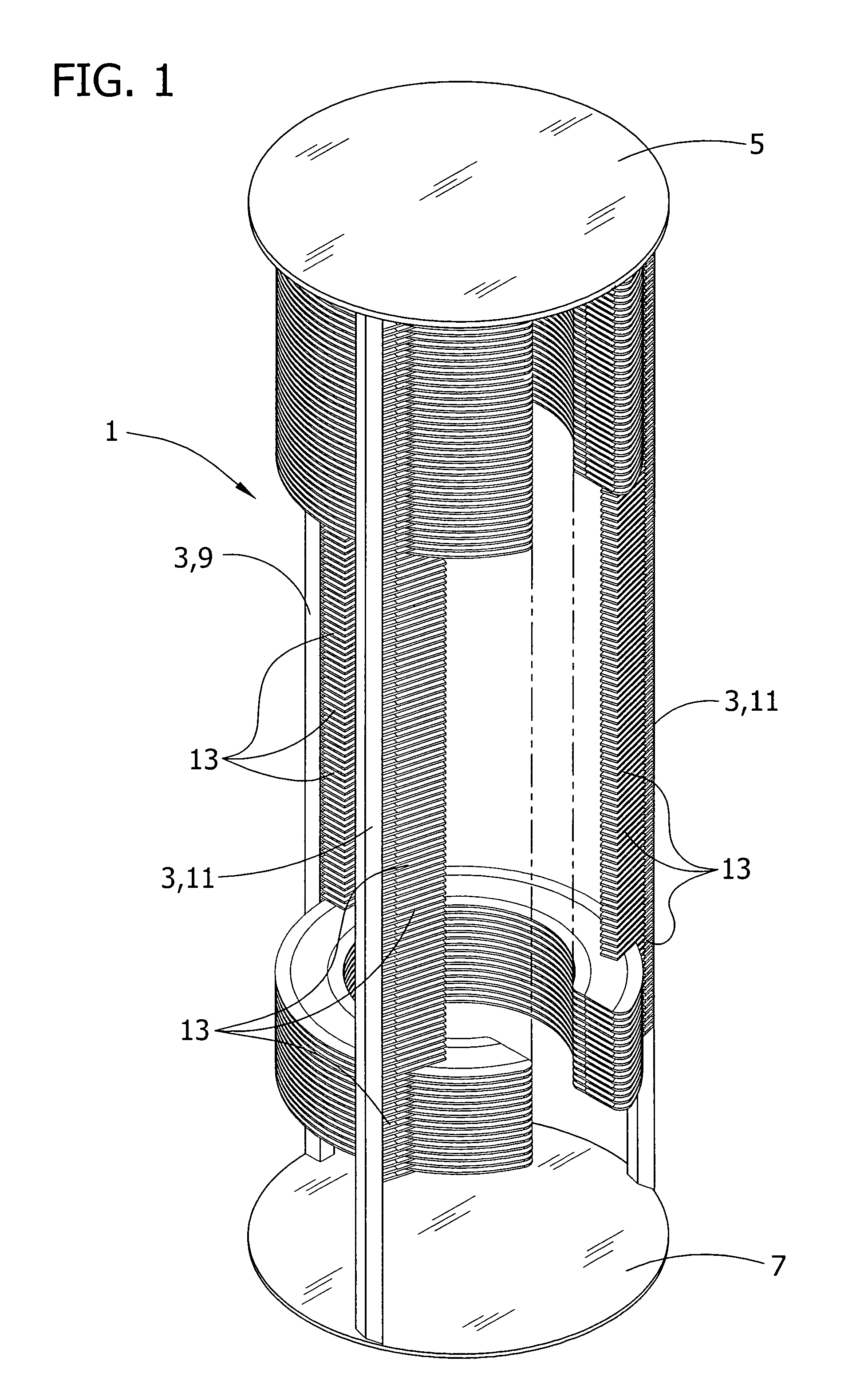
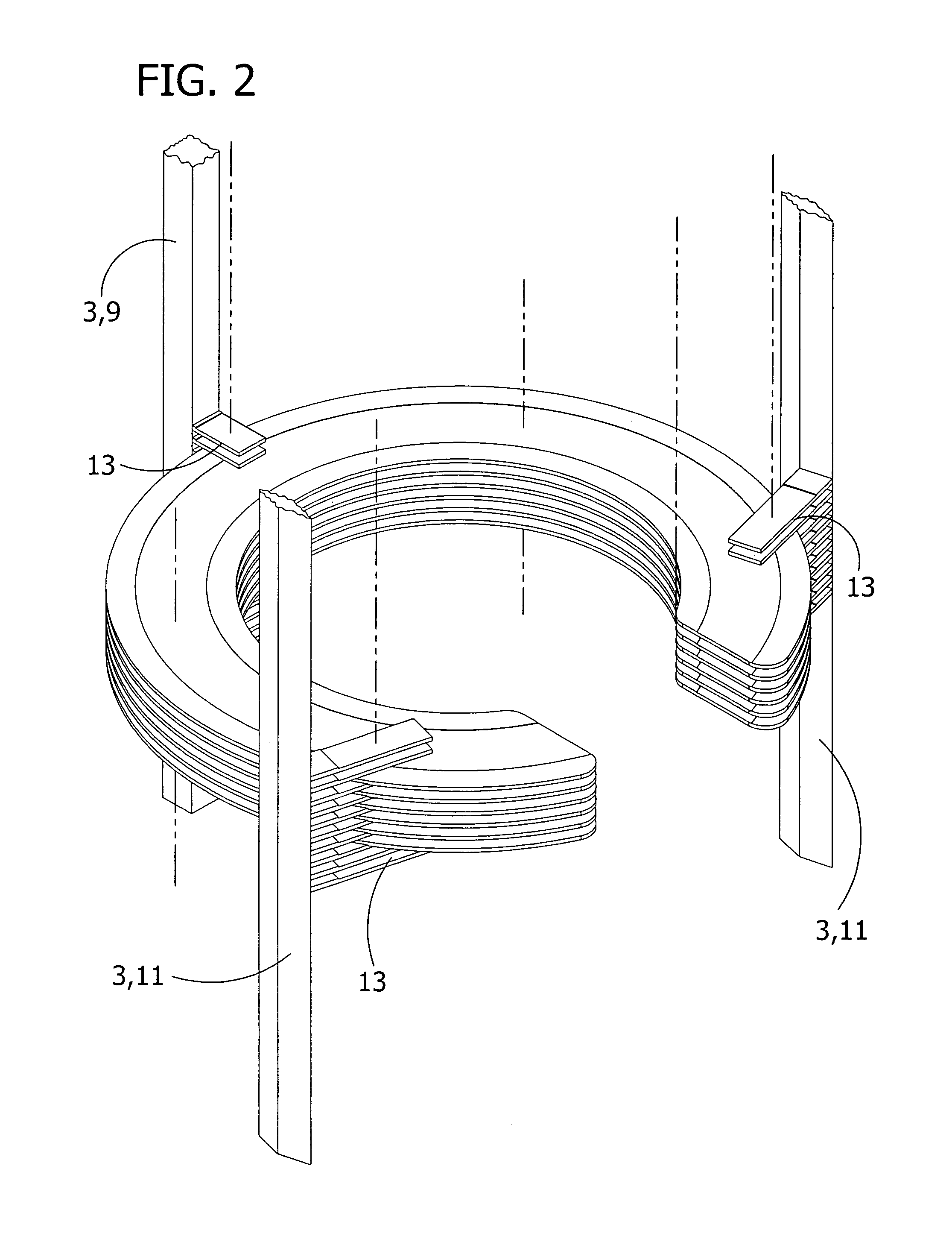
[0024]Referring now to the drawings and in particular to FIG. 1 which illustrates a semiconductor wafer boat, indicated generally at 1, constructed according to the principles of the present invention. The wafer boat 1 includes spaced-apart support rods 3 that are affixed to a top 5 and a base 7 of the boat to retain the positions of the rods relative to each other. When the wafer boat 1 is placed in a vertical furnace, the support rods 3 are generally vertical. In the illustrated embodiment, the wafer boat 1 has a central rod 9 and two forward rods 11.

[0025]The support rods 3 support laterally extending fingers 13. The fingers 13 may be integrally formed on the support rods 3. For example, cuts may be made in an elongate one-piece structure, forming the fingers 13. The fingers 13 of the wafer boat 1 are arranged in groups lying in different common generally horizontal planes along the vertical extent of the support rods 3.

[0026]Referring to FIG. 3, the fingers 13 that lie in a same...


PUM

PropertyMeasurementUnit
thicknessaaaaaaaaaa
thicknessaaaaaaaaaa
diameteraaaaaaaaaa

Abstract

A wafer boat for use in heat treatment of semiconductor wafers in a vertical furnace comprises support rods extending generally vertically when the wafer boat is placed in the vertical furnace. Fingers are supported by and extend along vertical extent of the support rods. Wafer holder platforms are adapted to be supported by groups of fingers lying in generally different common horizontal planes. The fingers are adapted to underlie the wafer holder platforms and support the platforms at the support locations. The fingers and wafer holder platforms each have a respective first overall maximum thickness. The support location of at least one of the fingers and the wafer holder platforms have a second maximum thickness less than the first overall maximum thickness.

Description

BACKGROUND OF THE INVENTION[0001]This invention relates generally to a semiconductor wafer boat, and more particularly, to an improved semiconductor wafer boat for use in heat treatment of semiconductor wafers in a vertical furnace.[0002]High temperature heat-treatment (annealing) of semiconductor wafers is commonly used to achieve certain desirable characteristics. For example, such a process may be used to create a defect free layer of silicon on the wafers. The high temperature annealing process of the type to which the present invention particularly relates is carried out in a vertical furnace which preferably subjects the wafers to temperatures above 1100 degrees C., and more preferably between about 1200 degrees C. and about 1300 degrees C.[0003]During high temperature heat-treatment, at temperatures above 750 C and especially above 1100 C, the silicon wafers become more plastic. If the silicon wafers are not adequately supported during heat treatment, the wafers may undergo s...

Claims


Application Information

Patent Timeline
Patent Type & Authority Patents(United States)
IPC IPC(8): F27D5/00
CPCC23C16/4583C30B25/12H01L21/67309F27D5/0037C30B31/14
Inventor GUPTA, PUNEETSHIVE, LARRY W.GILMORE, BRIAN L.
Owner GLOBALWAFERS CO LTD
Why Eureka
Try Eureka