Semiconductor device using a nitride semiconductor

a technology of nitride and semiconductor, applied in the direction of semiconductor/solid-state device manufacturing, semiconductor devices, semiconductor devices, etc., can solve the problems of schottky gate structure, leak current increase, device destruction,

Active Publication Date: 2006-05-02
KK TOSHIBA
View PDF7 Cites 142 Cited by
  • Summary
  • Abstract
  • Description
  • Claims
  • Application Information

AI Technical Summary

Problems solved by technology

However, in general, the Schottky gate structure has a problem that a leak current increases, when a gate leak current is large and device temperature rises.
A normally-on type device has a problem that a large current flows at the moment at which a power to a circuit is turned on, and this sometimes results in destruction of the device.

Method used


Image

  • Semiconductor device using a nitride semiconductor
  • Semiconductor device using a nitride semiconductor
  • Semiconductor device using a nitride semiconductor

Examples


first embodiment

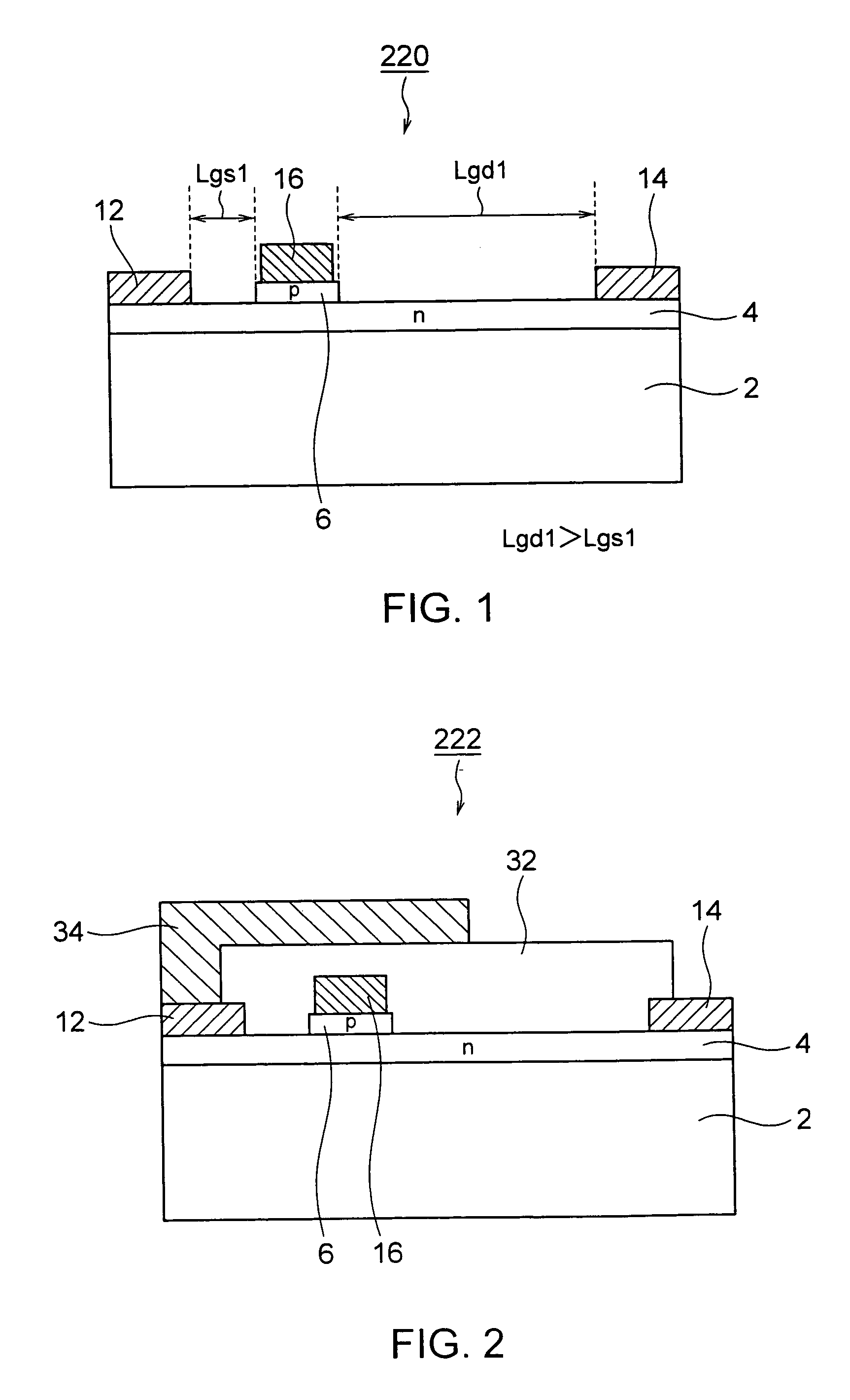
[0067]FIG. 1 is a sectional view schematically showing a first embodiment of a semiconductor device according to the present invention. A GaN heterostructure field effect transistor (hereinafter referred to simply as an HFET) 220 which is shown in FIG. 1 comprises a channel layer 2, an n-type barrier layer 4, a p-type base layer 6, a gate electrode 16, a source electrode 12, and a drain electrode 14. The channel layer 2 is formed of an i-GaN layer, and corresponds to a first semiconductor layer represented by, for example, a composition formula AlxGa1-xN (0≦x≦1). The n-type barrier layer 4 corresponds to a first conductivity type or non-doped second semiconductor layer represented by, for example, a composition formula AlyGa1-yN (0≦y≦1, x2 to supply an electron to a channel. Furthermore, the p-type base layer 6 is selectively formed of a p-GaN layer on the n-type barrier layer 4, and corresponds to a third semiconductor layer represented by, for example, the composition formula AlxG...

second embodiment

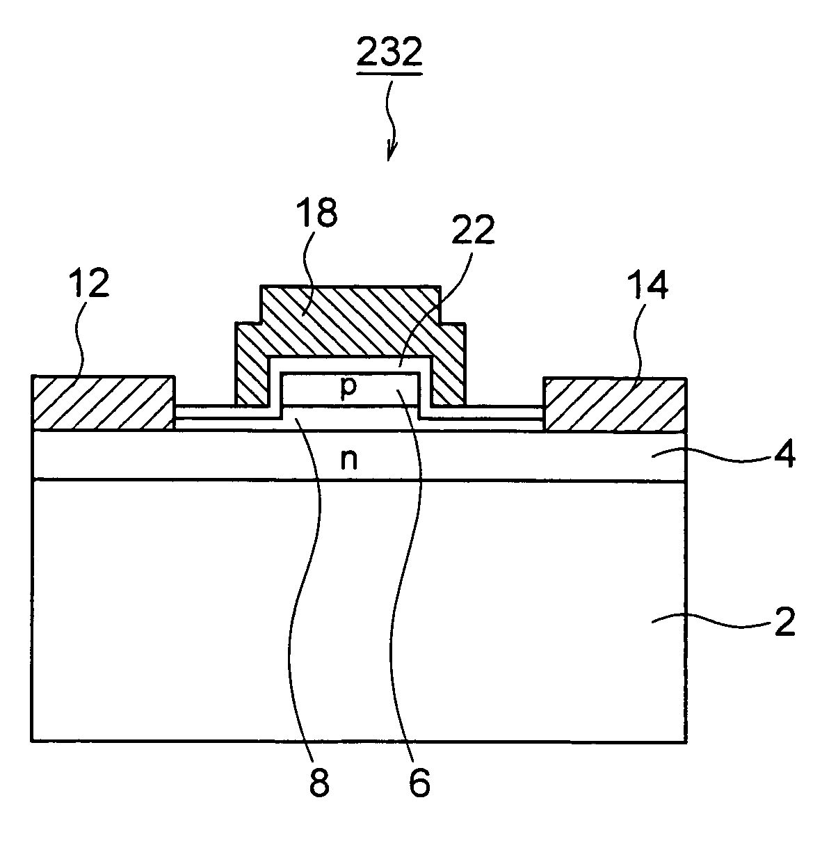
[0079]FIG. 4 is a sectional view schematically showing a second embodiment of a semiconductor device according to the present invention. A GaN insulating gate type heterostructure field effect transistor (hereinafter referred to simply as GaN-MIS-HFET) 230 shown in FIG. 4 further comprises a gate insulating film 22 formed so as to coat the barrier layer 4 and base layer 6, and an insulating gate (MIS gate) structure including a gate electrode 18 formed on the gate insulating film 22 instead of the gate electrode 16 of the GaN-HFET 220 shown in FIG. 1. The gate insulating film 22 can be formed of SiN, SiO2, Al2O3 or the like.

[0080]According to the present embodiment, it is possible to set a gate leak current substantially to zero by use of this MIS gate structure.

[0081]The other constitution of the GaN-MIS-HFET shown in FIG. 4 is substantially the same as that of the HFET 220 shown in FIG. 1. The 2DEG carrier concentration of the channel under the gate electrode when the gate voltage...

third embodiment

[0084]FIG. 6 is a sectional view schematically showing a third embodiment of a semiconductor device according to the present invention.

[0085]In a GaN-MIS-HFET 240 shown in FIG. 6, the interval Lgd between the gate electrode 18 and the drain electrode 14 is set to be larger than the interval Lgs between the gate electrode 18 and the source electrode 12. A high breakdown voltage is required for a power semiconductor device, and the breakdown voltage needs to be held between the gate and drain in the horizontal type device shown in FIG. 6. Therefore, when the distance between the gate and drain is lengthened, the breakdown voltage can be increased.

[0086]FIG. 7 is a sectional view schematically showing a modification of the GaN-MIS-HFET 240 shown in FIG. 6. A GaN-MIS-HFET 242 shown in FIG. 7 further comprises a first field insulating film 32 formed so as to coat the gate electrode, and a field plate electrode 38 formed on the field insulating film 32 and connected to the source electrod...


PUM


Abstract

A semiconductor device includes: a first semiconductor layer represented by a composition formula AlxGa1-xN (0≦x≦1) a first conductivity type or non-doped second semiconductor layer represented by a composition formula AlyGa1-yN (0≦y≦1, x<y) and formed on the first semiconductor layer; a second conductivity type third semiconductor layer represented by a composition formula AlxGa1-xN (0≦x≦1) and selectively formed on the second semiconductor layer; a gate electrode formed on the third semiconductor layer; a source electrode electrically connected to the second semiconductor layer; and a drain electrode electrically connected to the second semiconductor layer. The distance between the drain electrode and the third semiconductor layer is longer than the distance between the source electrode and the third semiconductor layer.

Description

CROSS REFERENCE TO RELATED APPLICATION[0001]This application claims benefit of priority under 35USC §119 to Japanese Patent Application No. 2004-54330, filed on Feb. 27, 2004, the contents of which are incorporated by reference herein.BACKGROUND OF THE INVENTION[0002]1. Field of the Invention[0003]The present invention relates to a semiconductor device, for example, to an insulating gate type field effect transistor using a nitride semiconductor.[0004]2. Related Background Art[0005]Since a nitride semiconductor device using gallium nitride (hereinafter referred to simply as GaN) has a large band gap as compared with a semiconductor device using silicon (Si), the semiconductor device has a high critical electric field, and from this characteristic, a small-sized device having a high breakdown voltage is easily realized. Accordingly, in a semiconductor for electric power control, a low on-resistance is achieved, and a device having a low loss can be realized. Above all, in a field eff...

Claims


Application Information

Patent Timeline
Patent Type & Authority Patents(United States)
IPC IPC(8): H01L31/072H01L29/808H01L21/336H01L21/337H01L21/338H01L29/20H01L29/778H01L29/78H01L29/812H01L31/109
CPCH01L29/1066H01L29/7787H01L29/432H01L29/7786H01L29/2003H01L29/402H01L29/4236
Inventor SAITO, WATARUOMURA, ICHIRO
Owner KK TOSHIBA
Why Eureka
Try Eureka