Light emitting device display circuit and drive method thereof

a technology of light emitting devices and display circuits, applied in the direction of instruments, computing, electric digital data processing, etc., can solve the problems of reducing device variation across, increasing device complexity, and substantial increase in the complexity of pixel circuits, so as to eliminate the dependence on threshold voltage variation and oled

Inactive Publication Date: 2006-05-30
CHOU CHEN JEAN
View PDF13 Cites 78 Cited by
  • Summary
  • Abstract
  • Description
  • Claims
  • Application Information

AI Technical Summary

Problems solved by technology

The major challenges in achieving such a commercialization include (1) improving the material and device operating life, and (2) reducing device variation across the display area.
As more elaborated control circuits being incorporated into individual pixels in these solutions, an inevitable consequence is an increase of device complexity.
Comparing to the basic pixel circuit in FIG. 2, it is evident that any current solution to the uniformity issue involves a substantial increase in the complexity of pixel circuit, and thus likelihood of reduction of available light emitting area, efficiency, and product yield.

Method used


Image

  • Light emitting device display circuit and drive method thereof
  • Light emitting device display circuit and drive method thereof
  • Light emitting device display circuit and drive method thereof

Examples


Embodiment Construction

[0032]This invention and the claimed subjects therein are directed to operating a display containing light emitting elements.

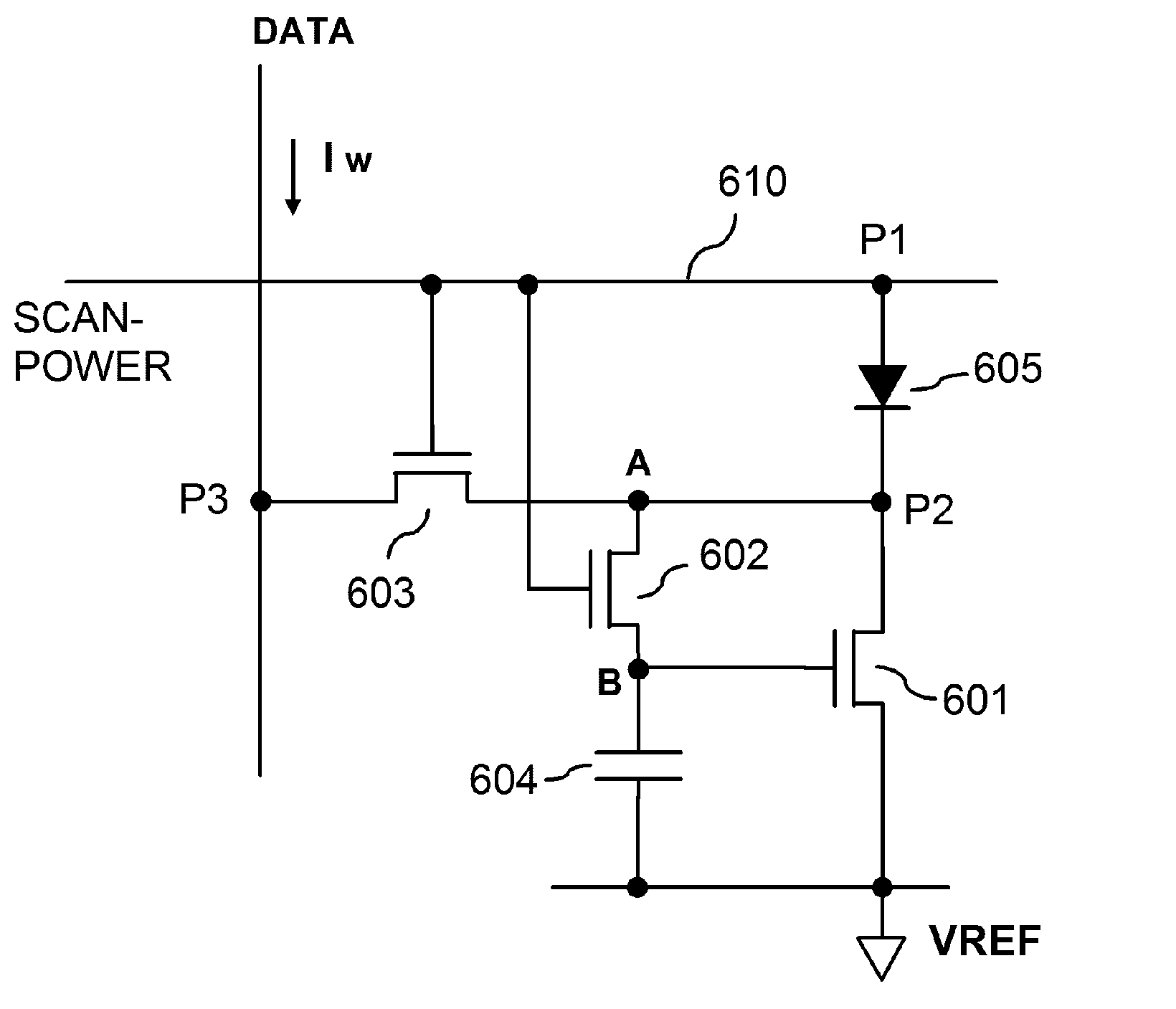
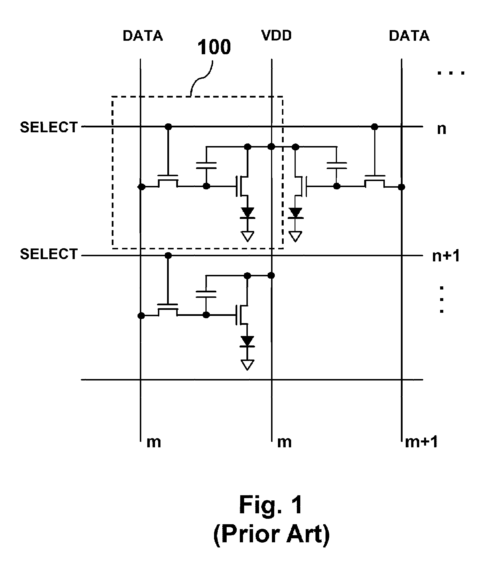
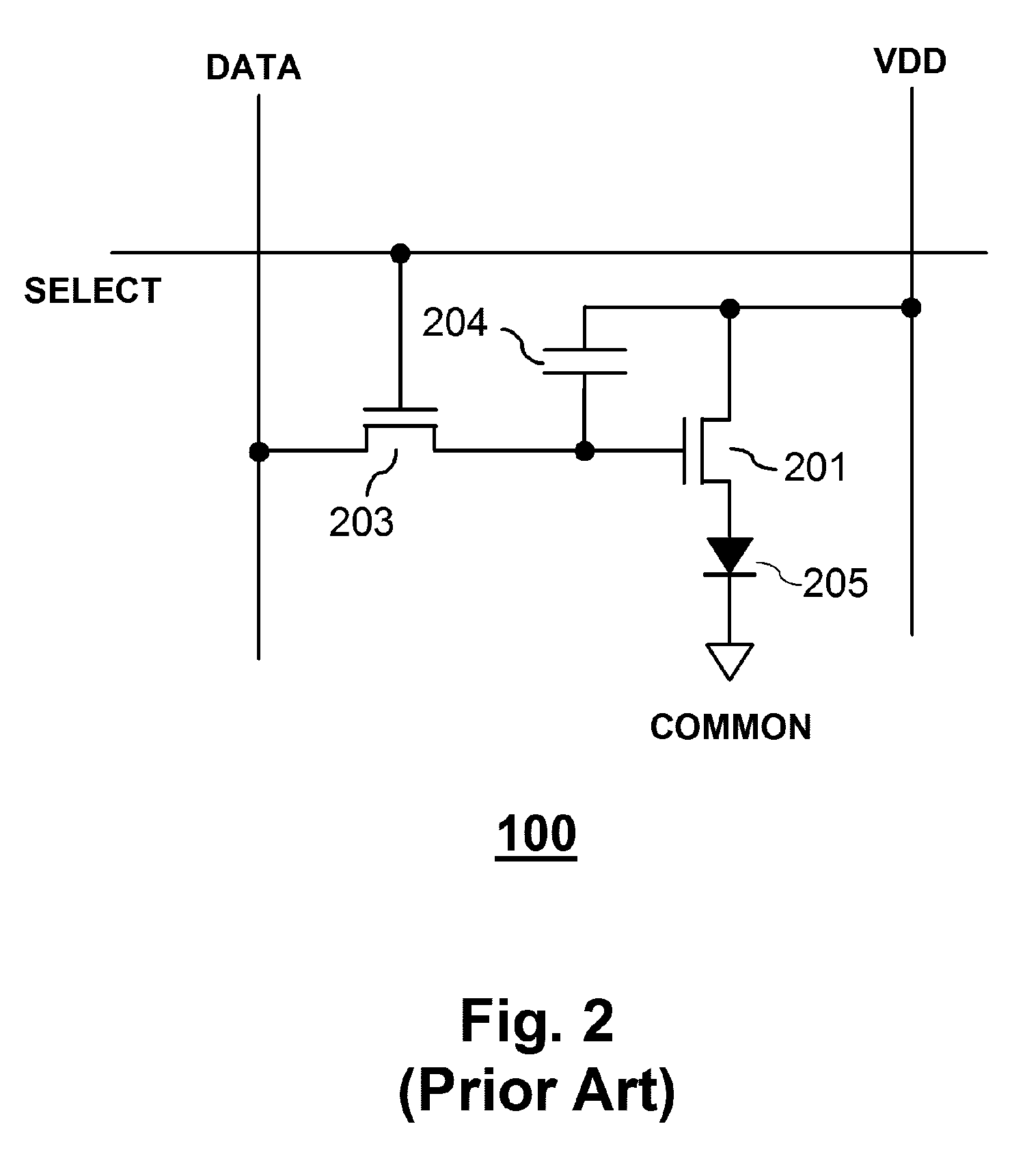
[0033]The present invention provides active matrix pixel circuits and a method to drive such. The circuit comprises two conducting channels in a pixel, enabled alternately by the signals applied to the same control electrode. Preferred embodiments of the present invention are provided for the current drive scheme to eliminate dependency on threshold voltage variation and OLED characteristics. The present invention also utilizes a drive method that merges conventional power delivering electrode and scanning electrode into a single access electrode (scan-power). Preferred embodiments in three transistor implementation are provided to illustrate the simplicity of the solutions for current drive scheme within the present invention. Additional embodiments are provided as illustration of the implementation principle.

[0034]Preferred embodiments of the present inventi...


PUM


Abstract

Multiple conducting channels in a display pixel, controlled by a single access electrode are provided in the present invention. Such pixel circuits operate to set a pixel data voltage by directing a data current to one of the conducting channels, while deliver a drive current to the light emitting device in a pixel via the other conducting channel. Current-controlled drive scheme, independent of threshold voltage, is achievable in the present invention without substantial increase in pixel complexity. Such merged pixel structures provide simplicity and greater flexibility in implementing current drive pixel structure.

Description

CROSS REFERENCE[0001]The present application claims priority of U.S. Provisional Patent Application No. 60 / 522,151, filed on Aug. 21, 2004, which is hereby incorporated by reference.BACKGROUND OF THE INVENTION[0002]1. Field of the Invention[0003]The present invention relates to the pixel circuits and drive method of an active matrix display comprising light-emitting devices which emits light by conducting a driving current through a light emitting material such as an organic semiconductor thin film. Such pixel circuits comprise active elements, such as thin film transistors, for controlling the light emitting operation of the respective light emitting devices. More specifically, the present invention provides pixel circuits comprising a multi-functional control electrode and a method to operate such pixel circuits. Furthermore, pixel circuits in the present invention are structured with alternating conducting channels, controlled by said multi-functional control electrodes. Pixel ci...

Claims


Application Information

Patent Timeline
Patent Type & Authority Patents(United States)
IPC IPC(8): G09G3/36
CPCG09G3/325G09G2300/0866G09G2300/0842
Inventor CHOU, CHEN-JEAN
Owner CHOU CHEN JEAN
Why Eureka
Try Eureka